LX1660 Ver la hoja de datos (PDF) - Microsemi Corporation
Número de pieza
componentes Descripción
Lista de partido
LX1660 Datasheet PDF : 15 Pages
| |||
PRODUCT DATABOOK 1996/1997
ADVANCED PWM CONTROLLER
PR O D U C T I O N D ATA S H E E T
LX1660/1661
USING THE LX1660/61 DEVICES
C7 HICCUP CAPACITOR SELECTION (continued)
The resulting time is the duration allowed for the 10% duty
cycle drive to be applied to the bottom switch (the top switch is
OFF during current limit). The OFF-time will be fixed at ten times
(10x) this number, and determines the time interval the supply
remains completely OFF until re-try. If the short has been
removed, the supply will resume normal operation. No power
cycling is necessary to reset the VRM module after a current limit
event.
As an example, if a 0.1µF hiccup capacitor is chosen, the
bottom switch drive will pulse at (approximately) a 10% duty cycle
for 10mA, when current limit is reached. It will then shut OFF for
100ms, at which time a re-try cycle is attempted, which will result
in either normal operation or another 10% duty cycle burst.
FET SELECTION
To insure reliable operation, the operating junction temperature
of the FET switches must be kept below certain limits. The Intel
specification states that 115°C maximum junction temperature
should be maintained with an ambient of 50°C. This is achieved
by properly derating the part, and by adequate heat sinking. One
of the most critical parameters for FET selection is the R
DS(ON)
resistance. This parameter directly contributes to the power
dissipation of the FET devices, and thus impacts heat sink design,
mechanical layout, and reliability. In general, the larger the
current handling capability of the FET, the lower the R will
DS(ON)
be, since more die area is available.
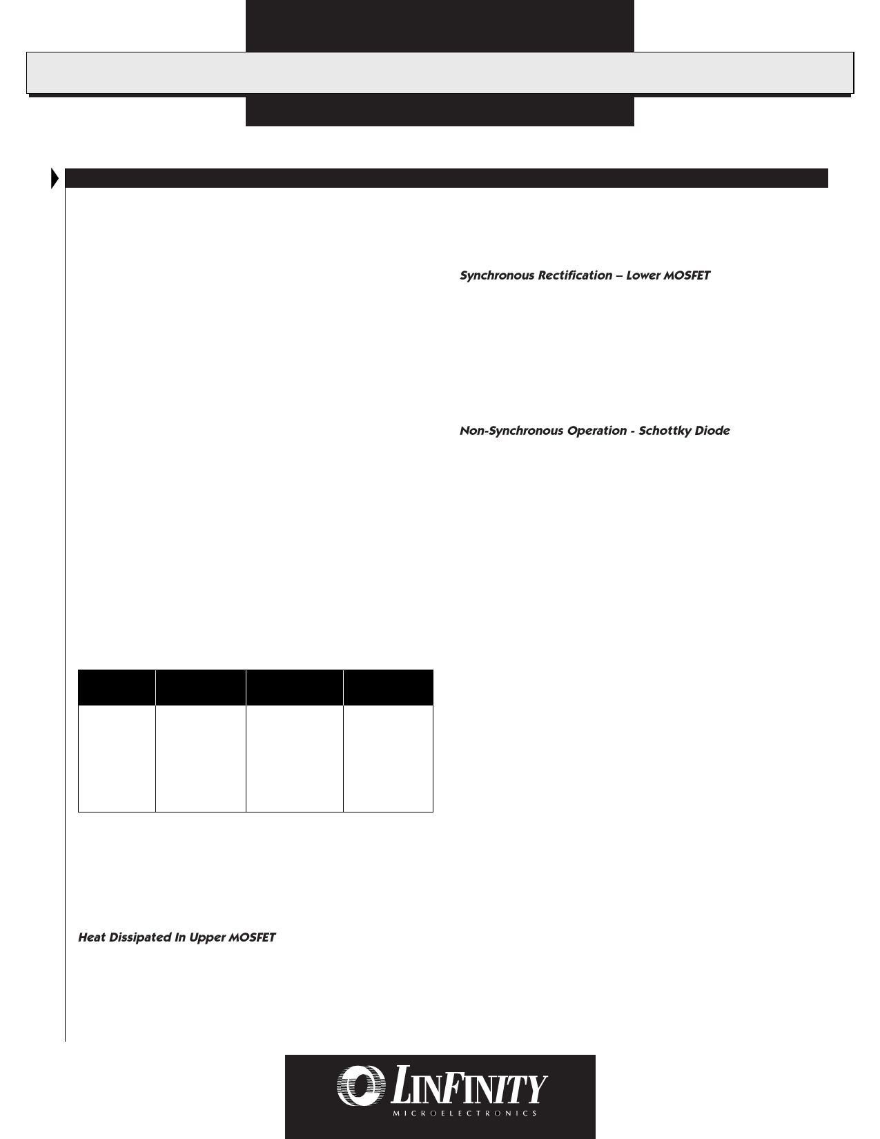
TABLE 4 - FET Selection Guide
This table gives selection of suitable FETs from International Rectifier.
Device
RDS(ON) @
10V (mΩ)
ID @
TC = 100°C
Max. Break-
down Voltage
IRL3803
6
83
30
IRL22203N
7
71
30
IRL3103
14
40
30
IRL3102
13
56
20
IRL3303
26
24
30
IRL2703
40
17
30
All devices in TO-220 package. For surface mount devices (TO-263 /
D2-Pak), add 'S' to part number, e.g. IRL3103S.
The recommended solution is to use IRL3102 for the high side
and IRL3303 for the low side FET, for the best combination of
cost and performance. Alternative FET’s from any manufacturer
could be used, provided they meet the same criteria for RDS(ON).
Heat Dissipated In Upper MOSFET
The heat dissipated in the top MOSFET will be:
P
D
=
(I2
*
R
DS(ON)
*
Duty
Cycle)
+
(0.5
*
I
*
V
IN
*
t
SW
*
f
S
)
where tSW is switching transition line for body diode (~100ns)
and f is the switching frequency.
S
FET SELECTION (continued)
For the IRL3102 (13mΩ R ), converting 5V to 2.8V at 14A
DS(ON)
will result in typical heat dissipation of 1.48W.
Synchronous Rectification – Lower MOSFET
The lower pass element can be either a MOSFET or a Schottky
diode. The use of a MOSFET (synchronous rectification) will
result in higher efficiency, but at higher cost than using a Schottky
diode (non-synchronous).
Power dissipated in the bottom MOSFET will be:
P
D
=
I2
*
R
DS(ON)
*
[1
-
Duty
Cycle]
=
2.24W
[IRL3303 or 1.12W for the IRL3102]
Non-Synchronous Operation - Schottky Diode
A typical Schottky diode, with a forward drop of 0.6V will dissi-
pate 0.6 * 14 * [1 – 2.8/5] = 3.7W (compared to the 1.1 to 2.2W
dissipated by a MOSFET under the same conditions). This power
loss becomes much more significant at lower duty cycles – syn-
chronous rectification is recommended especially when a 12V-
power input is used. The use of a dual Schottky diode in a single
TO-220 package (e.g. the MBR2535) helps improve thermal dis-
sipation.
MOSFET GATE BIAS
The power MOSFETs can be biased by one of two methods:
charge pump or 12V supply connected to VC1.
1) Charge Pump (Bootstrap)
When 12V is supplied to the drain of the MOSFET, as in
Figure 5 (option), the gate drive needs to be higher than 12V
in order to turn the MOSFET on. Capacitor C20 and diodes
D1 & D2 are used as a charge pump voltage doubling circuit
to raise the voltage of V so that the TDRV pin always
C1
provides a high enough voltage to turn on Q1. The 12V
supply must always be connected to VCC to provide power
for the IC itself, as well as gate drive for the bottom MOSFET.
2) 12V Supply
When 5V is supplied to the drain of Q1, a 12V supply should
be connected to both V and V .
CC
C1
CURRENT SHARE APPLICATION
Synchronous rectifier stages should not be paralleled unless they
are locked in at the same frequency, or undesirable current
sourcing/sinking could occur. If synchronization is not practical,
the next best alternative is to disable the synchronous (bottom)
switch. This is easily accomplished with the LX1660/61 by pulling
the SYNCEN pin HIGH. In most applications, a 5 to 6% reduction
in efficiency will result when the synchronous driver is disabled.
A Schottky diode of the proper voltage and current ratings should
be installed across the inactive FET to conduct the inductor
current.
Copyright © 1998
Rev. 1.1 7/98
13
Share Link: 