LX1660 Ver la hoja de datos (PDF) - Microsemi Corporation
Número de pieza
componentes Descripción
Lista de partido
LX1660 Datasheet PDF : 15 Pages
| |||
PRODUCT DATABOOK 1996/1997
LX1660/1661
ADVANCED PWM CONTROLLER
PRODUCTION DATA SHEET
USING THE LX1660/61 DEVICES
USING THE LX1660/1661 IN PROGRAMMABLE APPLICATIONS
The LX1660/61 device may be used in conjunction with the
LX1670 Programmable Reference to implement a high-perfor-
mance, digitally-controlled switched-mode power supply suitable
for Pentium Pro Processors and other advanced microprocessor-
based designs. The LX1670 incorporates a 5-bit equivalent DAC,
which can be programmed by the microprocessor’s Voltage
Identification Code (VID). The LX1670 then commands the
LX1660/61 to provide the required output voltage. System
protection functions such as over voltage, SCR drive, and power-
good detection are embedded within the LX1670 device. See
Figure 5.
LAYOUT GUIDELINES - THERMAL DESIGN (continued)
cases are well suited for this application, and are the preferred
packages. Remember to remove any conformal coating from all
exposed PC traces which are involved in heatsinking.
General Notes
As always, be sure to provide local capacitive de-coupling close
to the chip. Be sure use ground plane construction for all high-
frequency work. Use low ESR capacitors where justified, but be
alert for damping and ringing problems. High-frequency designs
demand careful routing and layout, and may require several
iterations to achieve desired performance levels.
PROGRAMMING THE OUTPUT VOLTAGE
Select the voltage divider R14 and R15 values as shown in the table
below, using 1% metal film resistors:
TABLE 5
Desired Converter VOUT R14 Value
2.8
806Ω
2.9
909Ω
3.0
1.0kΩ
3.1
1.10kΩ
3.2
1.21kΩ
3.3
1.30kΩ
3.4
1.40kΩ
3.5
1.50kΩ
R15 Value
2kΩ
2kΩ
2kΩ
2kΩ
2kΩ
2kΩ
2kΩ
2kΩ
If other V values are needed, the divider values may be
OUT
calculated as follows:
V = V (1 + R14/R15)
OUT
REF
where V = 2.0V. Note that resistor R4 is part of a filter
REF
element, and does not enter into the calculations.
Please refer to the Application Information schematic for
the reference designators and part locations.
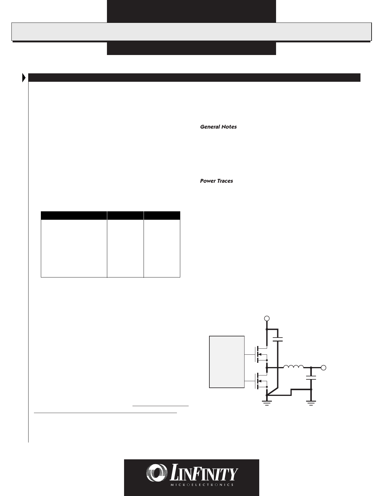
Power Traces
To reduce power losses due to ohmic resistance, careful consid-
eration should be given to the layout of traces that carry high
currents. The main paths to consider are:
s Input power from 5V supply to drain of top MOSFET.
s Trace between top MOSFET and lower MOSFET or Schottky
diode.
s Trace between lower MOSFET or Schottky diode and
ground.
s Trace between source of top MOSFET and inductor, sense
resistor and load.
All of these traces should be made as wide and thick as pos-
sible, in order to minimize resistance and hence power losses. It
is also recommended that, whenever possible, the ground, input
and output power signals should be on separate planes (PCB
layers). See Figure 10 – bold traces are power traces.
5V Input
LAYOUT GUIDELINES - THERMAL DESIGN
A great deal of time and effort were spent optimizing the thermal
design of the demo boards. Any user who intends to implement
an embedded motherboard would be well advised to carefully
read and follow these guidelines. If the FET switches have been
carefully selected, external heatsinking is generally not required.
However, this means that copper trace on the PC board must now
be used. This is a potential trouble spot; as much copper area as
possible must be dedicated to heatsinking the FET switches, and
the diode as well if a non-synchronous solution is used.
In our VRM module, heatsink area was taken from internal
ground and VCC planes which were actually split and connected
with VIAS to the power device tabs. The TO-220 and TO-263
LX166x
Output
FIGURE 10 — Power Traces
14
Copyright © 1998
Rev. 1.1 7/98
Share Link: 