IRFBC40AS Ver la hoja de datos (PDF) - International Rectifier
Número de pieza
componentes Descripción
Lista de partido
IRFBC40AS Datasheet PDF : 9 Pages
| |||
IRFBC40AS
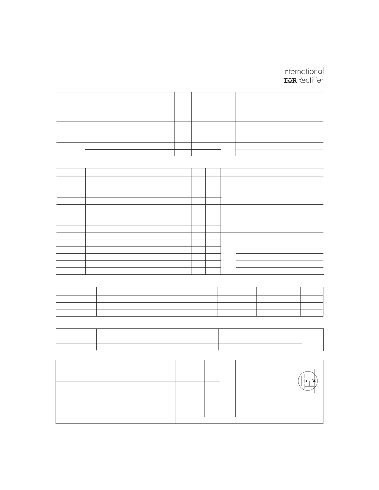
Static @ TJ = 25°C (unless otherwise specified)
Parameter
Min. Typ. Max. Units
Conditions
V(BR)DSS Drain-to-Source Breakdown Voltage 600
∆V(BR)DSS/∆TJ Breakdown Voltage Temp. Coefficient –––
RDS(on)
Static Drain-to-Source On-Resistance –––
VGS(th)
Gate Threshold Voltage
2.0
IDSS
Drain-to-Source Leakage Current
–––
–––
Gate-to-Source Forward Leakage
–––
IGSS
Gate-to-Source Reverse Leakage
–––
––– –––
0.66 –––
––– 1.2
––– 4.0
––– 25
––– 250
––– 100
––– -100
V VGS = 0V, ID = 250µA
V/°C Reference to 25°C, ID = 1mA
Ω VGS = 10V, ID = 3.7A
V VDS = VGS, ID = 250µA
µA VDS = 600V, VGS = 0V
VDS = 480V, VGS = 0V, TJ = 125°C
nA VGS = 30V
VGS = -30V
Dynamic @ TJ = 25°C (unless otherwise specified)
Parameter
Min. Typ. Max. Units
Conditions
gfs
Forward Transconductance
3.4 ––– ––– S VDS = 50V, ID = 3.7A
Qg
Total Gate Charge
––– ––– 42
ID = 6.2A
Qgs
Gate-to-Source Charge
––– ––– 10 nC VDS = 480V
Qgd
Gate-to-Drain ("Miller") Charge
––– ––– 20
VGS = 10V, See Fig. 6 and 13
td(on)
Turn-On Delay Time
––– 13 –––
VDD = 300V
tr
td(off)
tf
Rise Time
Turn-Off Delay Time
Fall Time
––– 23 ––– ns ID = 6.2A
––– 31 –––
RG = 9.1Ω
––– 18 –––
RD = 47Ω,See Fig. 10
Ciss
Input Capacitance
––– 1036 –––
VGS = 0V
Coss
Output Capacitance
––– 136 –––
VDS = 25V
Crss
Reverse Transfer Capacitance
––– 7.0 ––– pF ƒ = 1.0MHz, See Fig. 5
Coss
Output Capacitance
––– 1487 –––
VGS = 0V, VDS = 1.0V, ƒ = 1.0MHz
Coss
Coss eff.
Output Capacitance
Effective Output Capacitance
––– 36 –––
––– 48 –––
VGS = 0V, VDS = 480V, ƒ = 1.0MHz
VGS = 0V, VDS = 0V to 480V
Avalanche Characteristics
Parameter
EAS
Single Pulse Avalanche Energy
IAR
Avalanche Current
EAR
Repetitive Avalanche Energy
Typ.
–––
–––
–––
Max.
570
6.2
13
Units
mJ
A
mJ
Thermal Resistance
Parameter
Typ.
Max.
Units
RθJC
RθJA
Junction-to-Case
–––
Junction-to-Ambient ( PCB Mounted, steady-state)*
–––
1.0
°C/W
40
Diode Characteristics
Parameter
Min. Typ. Max. Units
Conditions
IS
Continuous Source Current
(Body Diode)
ISM
Pulsed Source Current
(Body Diode)
MOSFET symbol
D
––– ––– 6.2
A showing the
integral reverse
G
––– ––– 25
p-n junction diode.
S
VSD
Diode Forward Voltage
––– ––– 1.5 V TJ = 25°C, IS = 6.2A, VGS = 0V
trr
Reverse Recovery Time
Qrr
Reverse RecoveryCharge
ton
Forward Turn-On Time
2
––– 431 647 ns TJ = 25°C, IF = 6.2A
––– 1.8 2.8 µC di/dt = 100A/µs
Intrinsic turn-on time is negligible (turn-on is dominated by LS+LD)
www.irf.com
Share Link: 