IRCZ34 Ver la hoja de datos (PDF) - International Rectifier
Número de pieza
componentes Descripción
Lista de partido
IRCZ34 Datasheet PDF : 6 Pages
| |||
IRCZ34
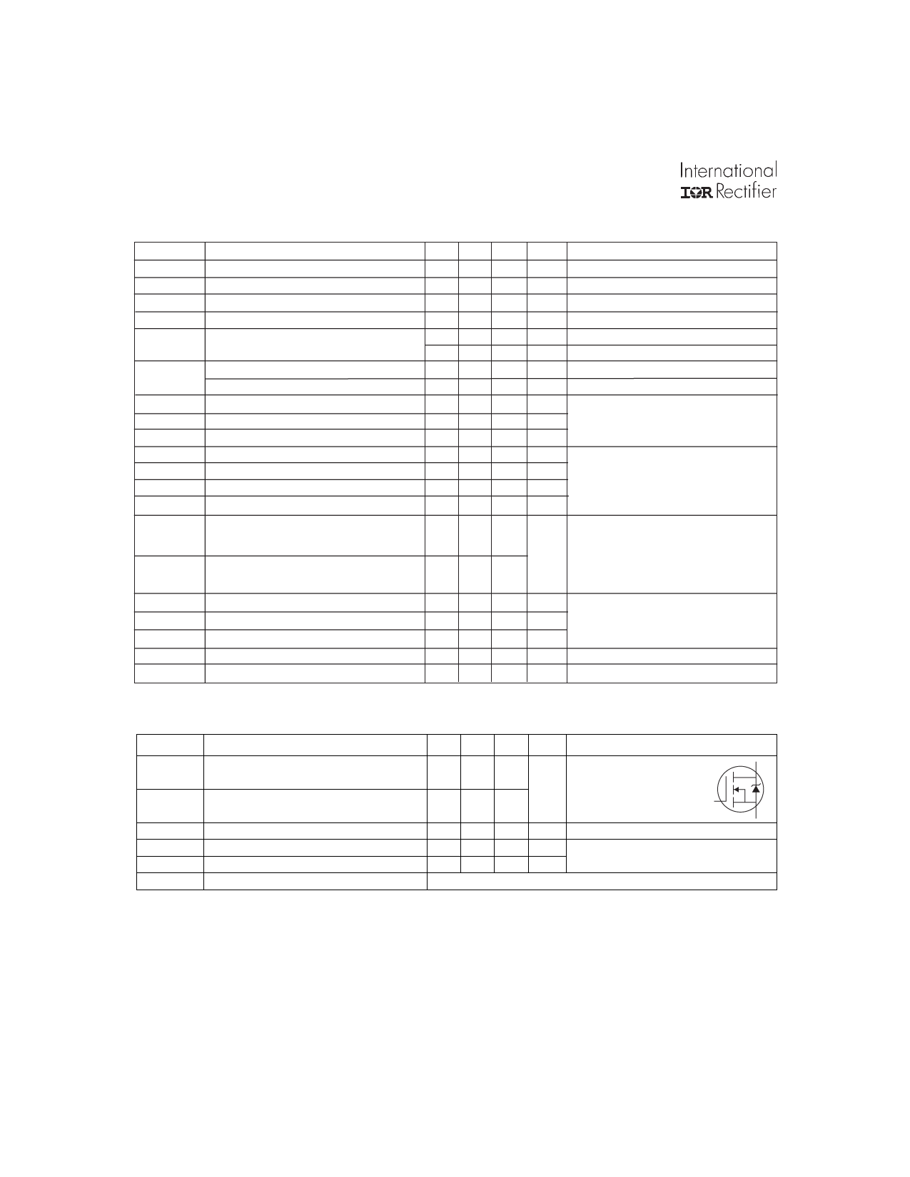
Electrical Characteristics @ TJ = 25°C (unless otherwise specified)
Parameter
V(BR)DSS Drain-to-Source Breakdown Voltage
∆V(BR)DSS/∆TJ Breakdown Voltage Temp. Coefficient
RDS(ON)
Static Drain-to-Source On-Resistance
VGS(th)
Gate Threshold Voltage
gfs
Forward Transconductance
IDSS
Drain-to-Source Leakage Current
IGSS
Qg
Qgs
Qgd
td(on)
tr
td(off)
tf
Gate-to-Source Forward Leakage
Gate-to-Source Reverse Leakage
Total Gate Charge
Gate-to-Source Charge
Gate-to-Drain ("Miller") Charge
Turn-On Delay Time
Rise Time
Turn-Off Delay Time
Fall Time
Min. Typ. Max. Units
Conditions
60 ––– ––– V VGS = 0V, ID = 250µA
––– 0.065 ––– V/°C Reference to 25°C, ID = 1mA
––– ––– 0.050 Ω VGS = 10V, ID = 18A
2.0 ––– 4.0 V VDS = VGS, ID = 250µA
9.4 ––– ––– S VDS = 25V, ID = 18A
––– ––– 25
VDS = 60V, VGS = 0V
––– ––– 250
VDS = 48V, VGS = 0V, TJ = 150°C
––– ––– 100
VGS = 20V
––– ––– -100
VGS = -20V
––– ––– 46
ID = 30A
––– ––– 11
––– ––– 22
nC VDS = 48V
VGS = 10V, See Fig. 6 and 13
––– 13 –––
VDD = 30V
––– 100 –––
––– 29 –––
––– 52 –––
ID = 30A
RG = 12Ω
RD = 1.0Ω, See Fig. 10
LD
Internal Drain Inductance
LC
Internal Source Inductance
––– 4.5 –––
––– 7.5 –––
Between lead,
6 mm (0.25 in.)
nH from package
and center of
die contact
Ciss
Input Capacitance
––– 1300 –––
VGS = 0V
Coss
Output Capacitance
––– 640 ––– pF VDS = 25V
Crss
Reverse Transfer Capacitance
––– 96 –––
ƒ = 1.0MHz, See Fig. 5
r
Current Sensing Ratio
1340 ––– 1480 ––– ID = 30A, VGS = 10V
Coss
Output Capacitance of Sensing Cells ––– 9.0 ––– pF VGS = 0V, VDS = 25V, ƒ = 1.0MHz
Source-Drain Ratings and Characteristics
Parameter
IS
Continuous Source Current
(Body Diode)
ISM
Pulsed Source Current
(Body Diode)
VSD
Diode Forward Voltage
trr
Reverse Recovery Time
Qrr
Reverse Recovery Charge
ton
Forward Turn-On Time
Min. Typ. Max. Units
Conditions
––– ––– 30
––– ––– 120
––– ––– 1.6
––– 120 230
––– 0.70 1.4
MOSFET symbol
D
showing the
A
integral reverse
G
p-n junction diode.
S
V TJ = 25°C, IS = 30A, VGS = 0V
ns TJ = 25°C, IF = 30A
nC di/dt = 100A/µs
Intrinsic turn-on time is negligible (turn-on is dominated by LS+LD)
Notes:
Repetitive rating; pulse width limited by
max. junction temperature. ( See fig. 11 )
ISD ≤ 30A, di/dt ≤ 200A/µs, VDD ≤ V(BR)DSS,
TJ ≤ 175°C
VDD = 25V, starting TJ = 25°C, L = 0.019mH
RG = 25Ω, IAS = 30A. (See Figure 12)
C-8
Pulse width ≤ 300µs; duty cycle ≤ 2%.
Share Link: 