P4C116 Ver la hoja de datos (PDF) - Semiconductor Corporation
Número de pieza
componentes Descripción
Lista de partido
P4C116 Datasheet PDF : 14 Pages
| |||
P4C116/P4C116L
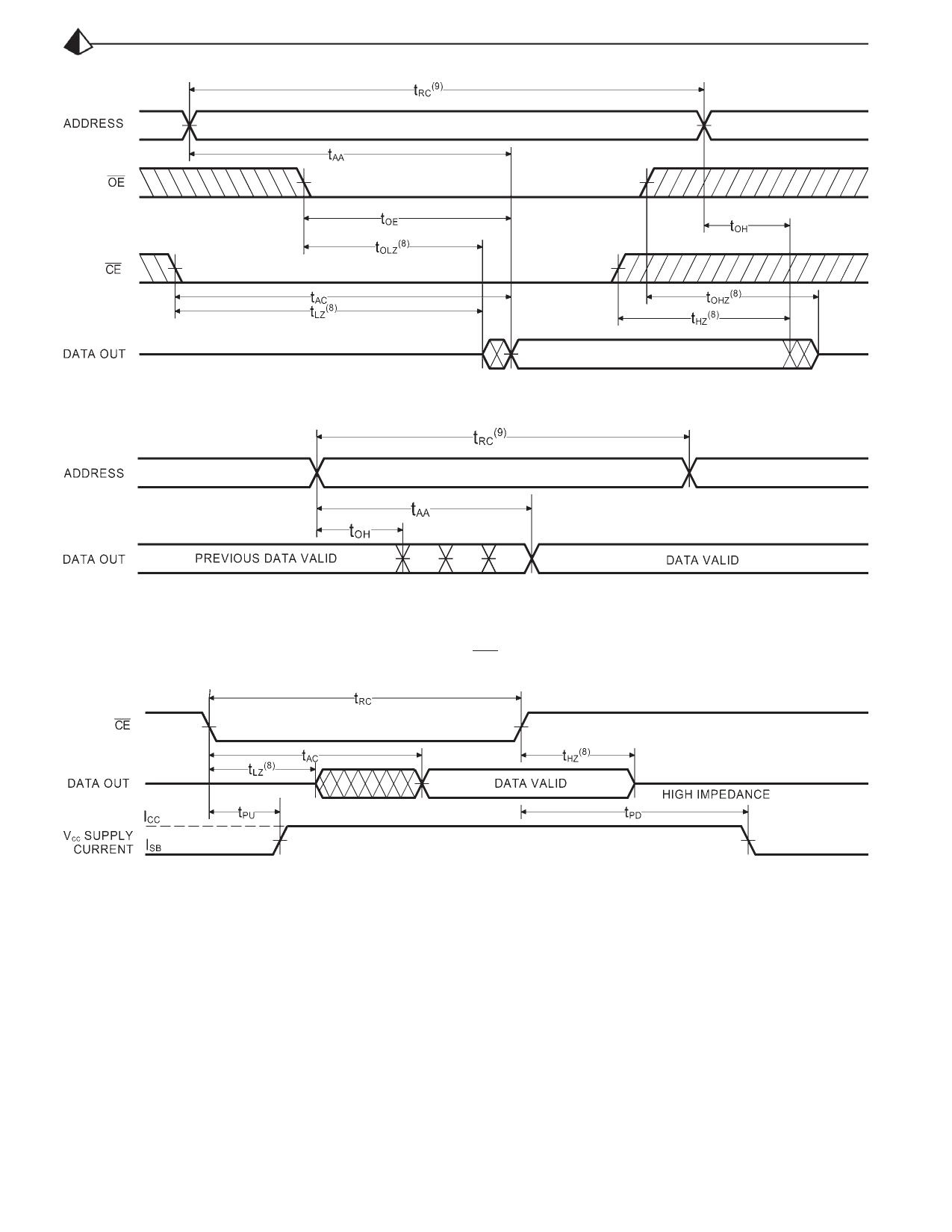
TIMING WAVEFORM OF READ CYCLE NO. 1 (OE CONTROLLED)(5)
TIMING WAVEFORM OF READ CYCLE NO. 2 (ADDRESS CONTROLLED)(5,6)
TIMING WAVEFORM OF READ CYCLE NO. 3 (CE CONTROLLED)(5,7)
Notes:
1. Stresses greater than those listed under MAXIMUM RATINGS may
cause permanent damage to the device. This is a stress rating only
and functional operation of the device at these or any other conditions
above those indicated in the operational sections of this specification
is not implied. Exposure to MAXIMUM rating conditions for extended
periods may affect reliability.
2. Extended temperature operation guaranteed with 400 linear feet per
minute of air flow.
3. Transient inputs with VIL and IIL not more negative than –3.0V and
–100mA, respectively, are permissible for pulse widths up to 20 ns.
4. This parameter is sampled and not 100% tested.
5. WE is HIGH for READ cycle.
6. CE is LOW and OE is LOW for READ cycle.
7. ADDRESS must be valid prior to, or coincident with CE transition
LOW.
8. Transition is measured ± 200 mV from steady state voltage prior to
change, with loading as specified in Figure 1. This parameter is
sampled and not 100% tested.
9. Read Cycle Time is measured from the last valid address to the first
transitioning address.
Document # SRAM110 REV A
Page 4 of 14
Share Link: 