RF2642PCBA-41X Ver la hoja de datos (PDF) - RF Micro Devices
Número de pieza
componentes Descripción
Lista de partido
RF2642PCBA-41X Datasheet PDF : 12 Pages
| |||
RF2642
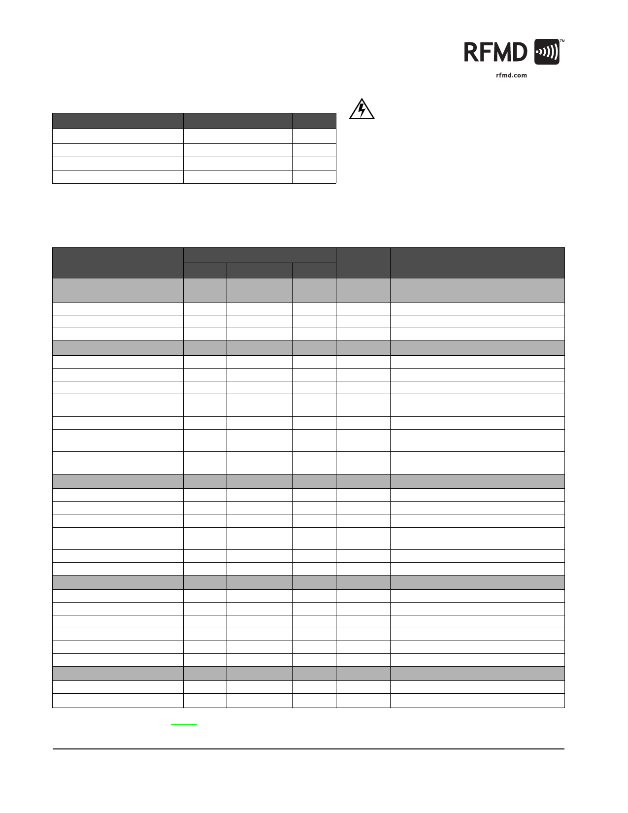
Absolute Maximum Ratings
Parameter
Supply Voltage
Input RF Power
Operating Ambient Temperature
Storage Temperature
Rating
-0.5 to +4.5
+3
-30 to +85
-30 to +150
Unit
VDC
dBm
°C
°C
Caution! ESD sensitive device.
Exceeding any one or a combination of the Absolute Maximum Rating conditions may
cause permanent damage to the device. Extended application of Absolute Maximum
Rating conditions to the device may reduce device reliability. Specified typical perfor-
mance or functional operation of the device under Absolute Maximum Rating condi-
tions is not implied.
RoHS status based on EUDirective2002/95/EC (at time of this document revision).
The information in this publication is believed to be accurate and reliable. However, no
responsibility is assumed by RF Micro Devices, Inc. ("RFMD") for its use, nor for any
infringement of patents, or other rights of third parties, resulting from its use. No
license is granted by implication or otherwise under any patent or patent rights of
RFMD. RFMD reserves the right to change component circuitry, recommended appli-
cation circuitry and specifications at any time without prior notice.
Parameter
Overall
RF Output Frequency Range
IF Frequency Range
Output Power
High Gain Mode
Gain
Noise Figure
IF Input Impedance
RF Output VSWR
Current Consumption
Adjacent Channel Power
Rejection (ACPR1)
Alternate Channel Power
Rejection (ACPR2)
Bypass Mode
Gain
Noise Figure
IF Input Impedance
RF Output VSWR
Output IP3
Current Consumption
LO Input
LO Frequency Range
LO Level
LO Input Impedance
LO to Mixer RF Output Leakage
LO Input VSWR
Power Supply
Voltage
Current Consumption
Specification
Min.
Typ.
Max.
824 to 849
130
+5
33
34.5
36
12
14
250
1.5
2:1
52
55
61
65
78
80
11.9
11.9
14
250
1.5
2:1
-4
+5.4
26
954 to 979
-6
-3
0
50
-33
-20
1.4
2:1
1.7
2:1
2.7
3.0
3.3
18
Unit
MHz
MHz
dBm
dB
dB
Ω
mA
dBc
dBc
dB
dB
Ω
dBm
mA
MHz
dBm
Ω
dBm
Condition
T=25°C, VCC=3.0V, RFOUT=830MHz,
LO=960MHz@-3dBm, IF=130MHz
CW
GAIN SELECT=2.7V, VPD=2.7V
Differential @ 130MHz
824MHz to 849MHz, external components
required
POUT=+5dBm, 885kHz offset
POUT=+5dBm, 1.98MHz offset
GAIN SELECT=0V, VPD=2.7V
Differential @ 130MHz
824MHz to 849MHz, external components
required
954MHz to 979MHz
GAIN SELECT=0V
GAIN SELECT=2.7V
V
mA
VPD = 0 V
NOTE: The measured results do not include the losses from the IF balun and SAW filter. On the evaluation board, those losses
are as follows: IF Balun=1dB, SAW Filter=2.5dB to 3.5dB.
2 of 12
7628 Thorndike Road, Greensboro, NC 27409-9421 · For sales or technical
support, contact RFMD at (+1) 336-678-5570 or sales-support@rfmd.com.
Rev A8 DS060925
Share Link: 