RF2642PCBA-41X Ver la hoja de datos (PDF) - RF Micro Devices
Número de pieza
componentes Descripción
Lista de partido
RF2642PCBA-41X Datasheet PDF : 12 Pages
| |||

RF2642
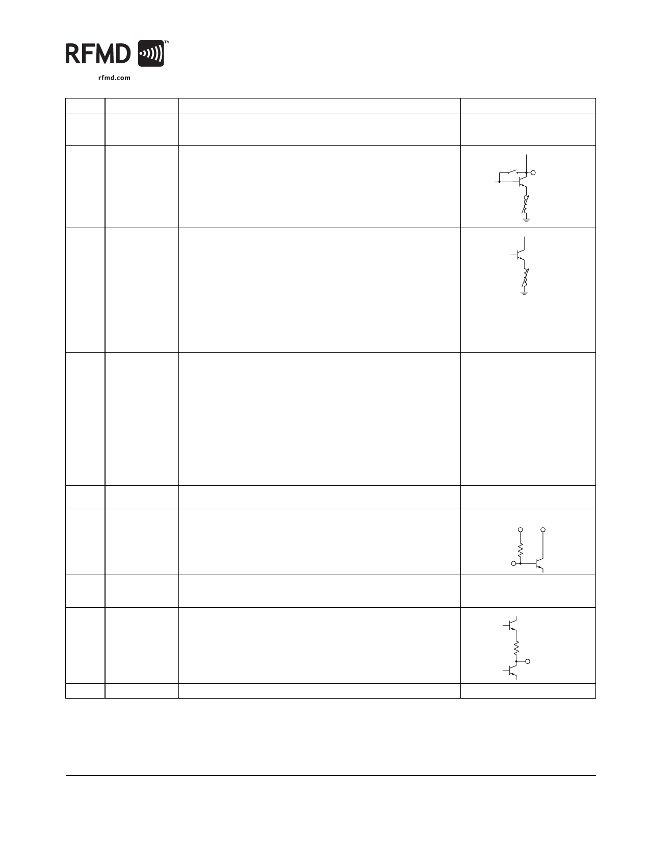
Pin Function Description
Interface Schematic
1
GND
Ground connection. For best performance, keep traces physically short
and connect immediately to ground plane. This pin is internally connected
to the die flag.
2
RF OUT
Output match of the second stage of the power amplifier driver. This ampli-
fier output pin is open collector. It is matched to 50Ω externally using a
simple LC match. Refer to the application schematic.
Gain
Select
RF OUT
3
RF GND2 The ground connection for the second stage of the power amplifier driver.
The inductance between this pin and the ground plane determines the
gain of the second stage. Increased inductance results in reduced gain.
On the evaluation board, the emitter ground inductance is set by the length
of the PCB trace connected between this pin and the ground. By sliding a
0Ω ground jumper along this line, the inductance, and hence the gain, may
be varied.
The evaluation board is shipped with the 0Ω jumper very close to the part,
resulting in minimum inductance, and therefore maximum second stage
gain. This translates to higher output IP3 and maximum ACPR1. This set-
ting results in performance 6dB better than the ACPR1 minimum specifica-
tion of 50dBc in the CDMA IS-95 specification for a POUT=+5dBm.
PCB
Trace
4
RF GND1 The ground connection for the first stage of the power amplifier driver. The See pin 3.
inductance between this pin and the ground plane determines the gain of
the first stage. Increased inductance results in reduced gain.
On the evaluation board, the emitter ground inductance is set by the length
of the PCB trace connected between this pin and the ground. By sliding a
0Ω ground jumper along this line, the inductance, and hence the gain, may
be varied.
The evaluation board is shipped with the 0Ω jumper far away from the
part, resulting in maximum inductance, and therefore minimum first stage
gain.
More gain may be obtained by shifting the 0Ω jumper toward the part. A
maximum total gain of 40dB may be achieved if the first stage is set to
minimum emitter inductor trace length.
5
VPA1
Power supply pin for the first stage power amplifier. External components
provide tuning for the interstage match.
6
RF IN
RF input to the power amplifier. This input is DC-coupled, so an external
blocking capacitor is needed if the pin is connected to a DC path.
Bias VPA1
7
PD
Power Down control When this pin is low, the amplifier section of the IC is
shut off. When this pin is high, the amplifier section of the IC is turned on.
The upconverter portion of the IC remains on regardless of the state of PD.
8
MIX OUT Output for the upconverting mixer. This input is DC-coupled, so an external
blocking capacitor is needed if the pin is connected to a DC path. The out-
put impedance is 50Ω.
9
GND
Same as pin 1.
RF IN
MIX OUT
Rev A8 DS060925
7628 Thorndike Road, Greensboro, NC 27409-9421 · For sales or technical
support, contact RFMD at (+1) 336-678-5570 or sales-support@rfmd.com.
3 of 12