A42U0616 Ver la hoja de datos (PDF) - AMIC Technology
Número de pieza
componentes Descripción
Lista de partido
A42U0616 Datasheet PDF : 25 Pages
| |||
A42U0616 Series
Absolute Maximum Ratings*
Input Voltage (Vin) . . . . . . . . . . . . . . . -0.5V to VCC+0.5V
Output Voltage (Vout) . . . . . . . . . . . . . -0.5V to VCC+0.5V
Power Supply Voltage (VCC) . . . . . . . -0.5V to VCC+0.5V
Operating Temperature (TOPR) . . . . . . . . . . 0°C to +70°C
Storage Temperature (TSTG) . . . . . . . . . -55°C to +150°C
Soldering Temperature X Time (TSOLDER) . . . . . . . . . . . . . .
. . . . . . . . . . . . . . . . . . . . . . . . . . . . . . . . . 260°C X 10sec
Power Dissipation (PD) . . . . . . . . . . . . . . . . . . . . . . . . 1W
Short Circuit Output Current (Iout) . . . . . . . . . . . . . . 50mA
Latch-up Current . . . . . . . . . . . . . . . . . . . . . . . . . . 200mA
*Comments
Stresses above those listed under "Absolute Maximum
Ratings" may cause permanent damage to this device.
These are stress ratings only. Functional operation of
this device at these or any other conditions above
those indicated in the operational sections of these
specification is not implied or intended. Exposure to
the absolute maximum rating conditions for extended
periods may affect device reliability.
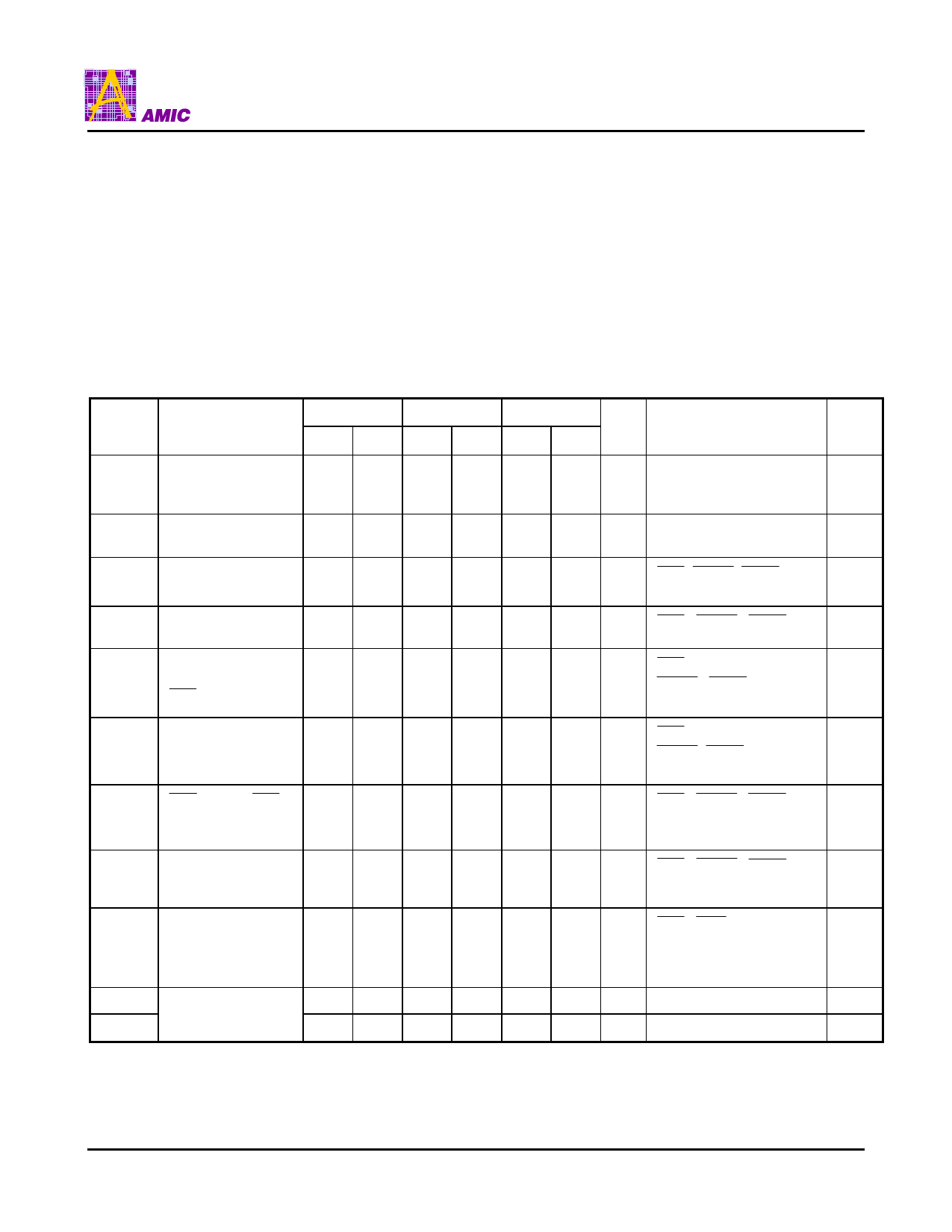
DC Electrical Characteristics (VCC = 2.5V ± 10%, VSS = 0V, Ta = 0°C to +70°C)
Symbol
Parameter
IIL
Input Leakage
Current
IOL Output Leakage
Current
ICC1 Operating Power
Supply Current
ICC2 TTL Standby Power
Supply Current
ICC3 Average Power
Supply Current,
RAS Refresh Mode
ICC4 EDO Page Mode
Average Power
Supply Current
ICC5
CAS -before- RAS
Refresh Power
Supply Current
ICC6 CMOS Standby
Power Supply
Current
ICC7 Self Refresh Mode
Current
VOH
Output Voltage
VOL
-50
-60
Min. Max. Min. Max.
-5 +5 -5 +5
-5 +5 -5 +5
- 120 - 110
-
1
-
1
- 120 - 110
- 100 -
90
- 110 - 100
-
0.2
-
0.2
- 250 - 250
2.0
-
2.0
-
-
0.4
-
0.4
-80
Min. Max.
-5 +5
-5 +5
- 100
-
1
Unit
µA
µA
mA
mA
Test Conditions
0V ≤ Vin ≤ Vin + 0.2V
Pins not under
Test = 0V
DOUT disabled,
0V ≤ Vout ≤ + VCC
RAS ,UCAS ,LCAS
Address cycling; tRC = min.
RAS =UCAS =LCAS =VIH
Notes
1, 2
-
100 mA RAS cycling,
1
UCAS =LCAS = VIH,
tRC = min.
-
80 mA RAS = VIL,
1, 2
UCAS ,LCAS Address
cycling; tPC = min.
-
90 mA RAS , UCAS , LCAS
1
cycling; tRC = min.
-
0.2 mA RAS =UCAS =LCAS =
VCC - 0.2V
-
250 µA RAS = CAS ≤ VSS+0.2V
All other input high levels
are VCC-0.2V or input low
levels are VSS +0.2V
2.0
-
V IOUT = -2mA
-
0.4
V IOUT = 2mA
PRELIMINARY (June, 2001, Version 0.0)
5
AMIC Technology, Inc.
Share Link: 