SA900 Ver la hoja de datos (PDF) - Philips Electronics
Número de pieza
componentes Descripción
Lista de partido
SA900 Datasheet PDF : 20 Pages
| |||
Philips Semiconductors
I/Q transmit modulator
Preliminary specification
SA900
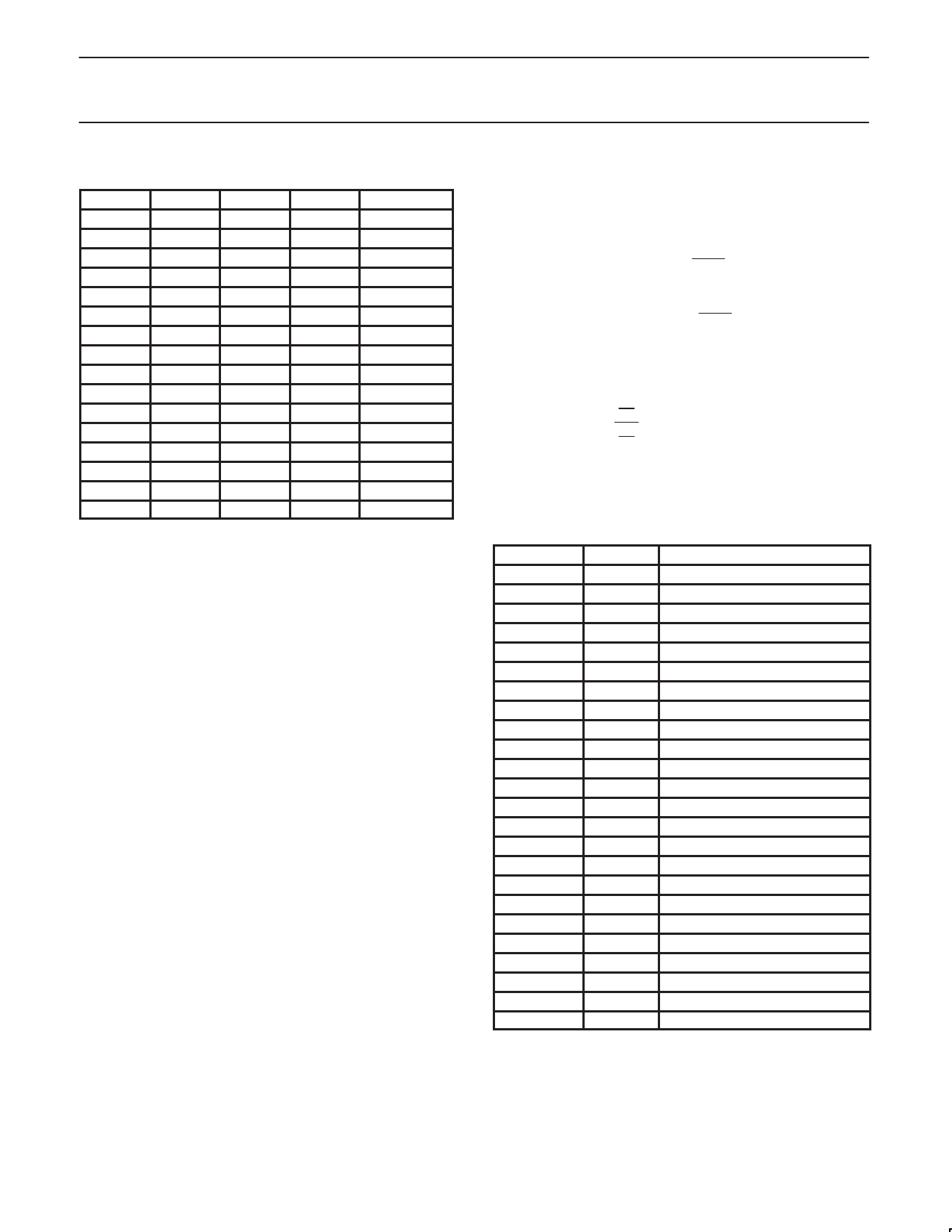
Table 1. VGA Power Control Limits
VGA
0
1
2
3
4
5
6
7
15
23
31
39
47
55
63
63
Min.
0
-1
-1
-1
-1
-1
-1
-1
-6.6
-6.6
-6.6
-6.6
-6.6
-6.6
-6.6
-43.2
Typ.
0
-.63
-.63
-.63
-.63
-.63
-.63
-.63
-5
-5
-5
-5
-5
-5
-5
-40.4
Max.
0
-.2
-.2
-.2
-.2
-.2
-.2
-.2
-3
-3
-3
-3
-3
-3
-3
-37.2
1. Guaranteed to be monotonic.
Relative VGA
0
0
1
2
3
4
5
6
7
15
23
31
39
47
55
0
AMPS Mode Operation
The SA900 can be configured to operate in the AMPS mode, where
FM modulation is applied to the SA900’s VCO. For the AMPS
mode, the VCO is configured with the proper synthesizer bandwidth
to allow the application of the AMPS modulation to the VCO varactor
tuned tank circuit. The modulated VCO signal is input into an image
reject mixer along with the TXLO signal, where the upper sideband
is rejected. This single sideband modulated signal then drives the
AMPS output power amplifier. The PA provides +2dBm power level
into 50Ω, with no external matching components required. The AD
(AMPS/DUAL) and the SE (synthesizer enable) bit control the power
up/down of the AMPS mode function. The transition of the TXEN
signal from low to high turns on the modulator. The falling edge of
TXEN signal disables the synthesizer and the modulator.
Synthesizer Operation
The SA900 synthesizer is comprised of the differential VCO circuit,
with external tank components, the Gilbert cell multiplier phase
detector with programmable charge pump current, crystal oscillator
and programmable prescalers. The charge pump output drives an
external second order loop filter. The output of the loop filter is used
to provide the control voltage to the VCO tuning varactor to
complete the PLL synthesizer. The synthesized VCO output
frequency is mixed with the TXLO signal to generate the transmit LO
from the lower sideband (the difference of the VCO and TXLO
frequencies). The output of VCO is fed to a programmable /N
prescaler with user selectable divides of 6, 7, 8 and 9 (all divides
configured to provide 50% duty cycle). The output of the /N divider
drives the A8/1 prescaler. The A8/1 divide is selected by the AD
control bit (AD=1 for /1, and AD=0 for /8). The output of the divide
A8/1 is fed into one input of the phase detector. The reference input
for the phase comparator is generated from the crystal oscillator
(XO) output from the B8/1 prescaler. The B8/1 divide is selected by
the AD control bit (AD=0 for /8, and AD=1 for /1). The phase
detector compares the prescaled XO reference phase to the VCO
prescaled phase, to generate a charge pump output current
proportional to the phase error. The phase detector, a Gilbert cell
multiplier type, having a linear output from 0 to π (π/2 ± π/2). The
charge pump peak output current is programmable from 100µA for
the AMPS mode (AD=0) to a maximum of 6.4mA for the DUAL
mode (AD=1) by way of an external current setting resistor placed
from IPEAK to circuit ground. The typical loop filter network is shown
in Figure 5. The charge pump current output is programmed by
AD + 0
ǒ Ǔ IOUT + 6 @
1.25V
RSET
AD + 1
ǒ Ǔ IOUT + 24 @
1.25V
RSET
where RSET is placed between IPEAK and GROUND.
The PLL frequency is determined by
VCO
+
XO
@
N
@
(A18)
(B18)
where N=6, 7, 8, 9 and A8/1 and B8/1 are controlled by the AD bit
(AD=1 A8/1 and B8/1 are divide by 1, AD=0 A8/1 and B8/1 are
divide 8).
Table 2. Data Word Format
Mnemonics
Bits
Function
A0
1 (MSB) Address bit 0 (1)
A1
2
Address bit 1 (0)
A2
3
Address bit 2 (1)
A3
4
Address bit 4 (1)
PC0
5
Power control bit 0
PC1
6
Power control bit 1
PC2
7
Power control bit 2
PC3
8
Power control bit 3
PC4
9
Power control bit 4
PC5
10
Power control bit 5
N0
11
Divide N bit 0
N1
12
Divide N bit 1
AD
13
AMPS/DUAL mode select bit
SE
14
Synthesizer enable bit
NA
15
NA
SM1
16
Sleep mode 1 control bit
SM2
17
Sleep mode 2 control bit
X
18
Divide 3/1 control bit
Y
19
Divide 2/1 control bit
NA
20
NA
NA
21
NA
NA
22
NA
NA
23
NA
NA
24 (LSB) NA
VCO Operation
The VCO is designed to operate from 90MHz to 140MHz. The VCO
tank is configured using a parallel inductor and a dual common
cathode tuning varactor diodes. DC blocking capacitors are used to
isolate the varactor
1997 Sept 16
10
Share Link: 