SA900 Ver la hoja de datos (PDF) - Philips Electronics
Número de pieza
componentes Descripción
Lista de partido
SA900 Datasheet PDF : 20 Pages
| |||
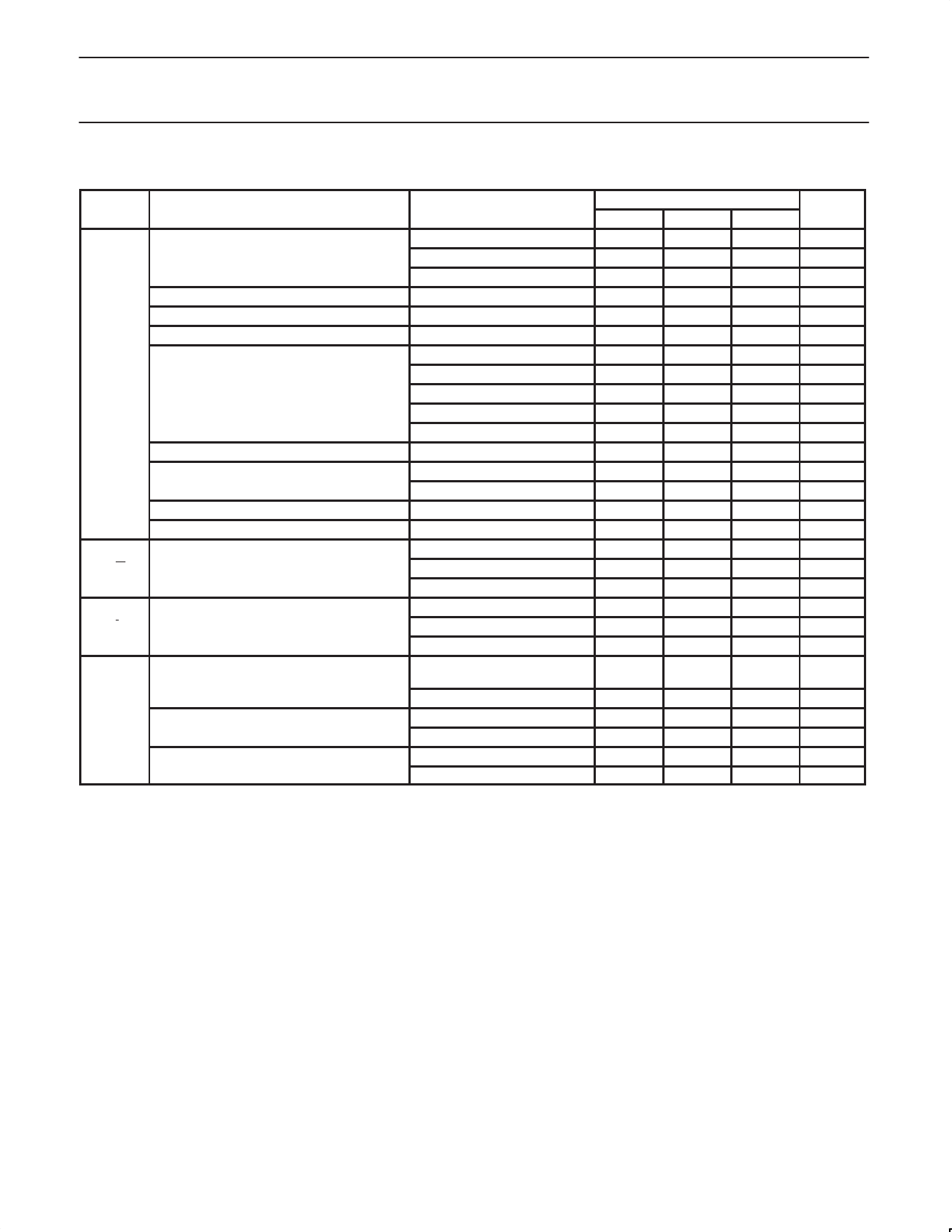
Philips Semiconductors
I/Q transmit modulator
Preliminary specification
SA900
AC ELECTRICAL CHARACTERISTICS (continued)
SYMBOL PARAMETER
TEST CONDITIONS
LIMITS
MIN
TYP
DUALTX
3rd order
-35
-42
(cont.) Linearity (0dB VGA, I and Q inphase)
5th order
-55
7th order
-65
Carrier suppression (I and Q quadrature)
VGA = 0dB
-35
-45
Carrier suppression (I and Q quadrature)
VGA = –40dB
-28
-33
Sideband suppression
I and Q quadrature
-35
-45
869 to 894MHz
–104
824 to 849MHz
–47
Spurious output
2 to 824MHz
–41
849 to 869MHz
–41
894MHz to 8.49GHz
–41
TXLO and harmonics
–21
Broadband noise (0dB VGA)
869 to 894MHz
935 to 960MHz
–136
–136
Adjacent channel noise power
@30kHz
–95
Alternate channel noise power
@60kHz
–101
Q/Q Baseband quadrature differential input
Max frequency
0.8
Differential modulation level
0.61
0.8
Differential input impedance
101
I/I
Baseband inphase differential input
Max frequency
0.8
Differential modulation level
0.61
0.8
Differential input impedance
10
Buffered TXLO differential outputs (AC
coupled)
Frequency range
900
VSWR (single-ended)
2:1
LO_1/2 Output impedance
single-ended
50
differential
100
Output level
single-ended, 50Ω
differential, 100Ω
50
90
100
180
NOTES:
1. Guaranteed by design.
2. Needs a different matching component. Max test frequency is 850MHz with test circuit shown in Figure 11.
MAX
21
1.01
21
1.01
1040
UNITS
dBc
dBc
dBc
dBc
dBc
dBc
dBm
dBc
dBc
dBc
dBc
dBc
dBm/Hz
dBm/Hz
dBc/Hz
dBc/Hz
MHz
VP-P
kΩ
MHz
VP-P
kΩ
MHz
Ω
Ω
mVP-P
mVP-P
FUNCTIONAL DESCRIPTION
Dual Mode Operation
The SA900 transmit modulator provides direct single sideband
quadrature modulation of the difference of the TXLO and VCO
frequencies, while providing quadrature LO signals for the I/Q
modulator. The quadrature LO signals are modulated with high
linearity by the baseband inphase (I) and quadrature (Q) signals.
The summed modulator output produces the lower sideband, while
rejecting the upper sideband. The I and Q inputs also provide DC
biasing for the modulator inputs. The summed output of the
modulator goes to a variable gain amplifier (VGA) to control the
output level, it has 40.0dB of attenuation control range, with 0.63dB
steps. The power control function is programmed by means of a
6-bit word (see Table 3). The VGA output drives the power amp
output stage to provide +2dBm average minimum power level (at
0dB power control) into 50Ω, in conjunction with external matching
components on DUALTX. The AD (AMPS/DUAL) and the SE
(synthesizer enable) bit control the power up/down of the DUAL
mode function. The transition of the TXEN, from low to high turns
on the modulator. The falling edge of the TXEN signal disables the
synthesizer and modulator. The TXLO is a system supplied LO
signal. The SA900 buffers the TXLO signal (LO_1/2) for use with
the system synthesizer (such as the SA7025) to form the system LO
synthesizer loop. The DUAL mode can also be used for AMPS
operation. The AMPS and DUAL mode modulation is generated by
the system DSP IC to provide the required I/Q baseband modulation
for the SA900. The DUAL output provides low broadband noise
output power (so that the receiver sensitivity is not degraded) and
high linearity to meet cellular phone system needs. Table 1 provides
the VGA power control limits.
The SA900 DUALTX output is externally matched with either a shunt
inductor to VCC and a series capacitor or a shunt inductor to VCC
and a series inductor. This matches the DUALTX output to 50Ω.
Values of the matching components are dependent on PCB layout,
typical values are shown in Figure 9.
1997 Sept 16
9
Share Link: 