IMIC9835CY Ver la hoja de datos (PDF) - Cypress Semiconductor
Número de pieza
componentes Descripción
Lista de partido
IMIC9835CY
Cypress Semiconductor

IMIC9835CY Datasheet PDF : 18 Pages
| |||
C9835
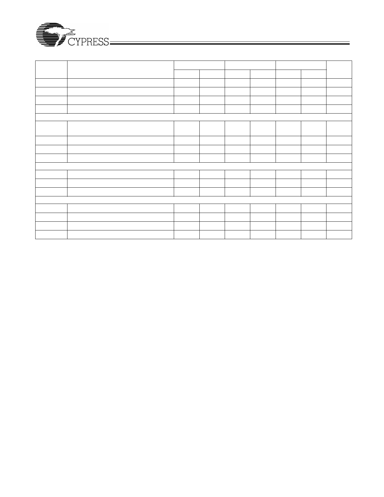
AC Parameters (continued)
Parameter
Description
TLOW
Tr / Tf
TSKEW
TCCJ
PCI(_F, 1:6) low time[31]
PCI(_F, 1:6) rise and fall times[27]
(Any PCI) to (Any PCI) Skew[26,29]
PCI(_F, 1:6) Cycle to Cycle Jitter[26,29]
DOT and USB
TPeriod
DOT and USB (48M[0,1]) period
(conforms to +167 ppm max) [25,26]
Tr / Tf
DOT and USB rise and fall times[27]
TCCJ
DOT and USB Cycle to Cycle Jitter[26,29]
TCCJ
VCH_CLK Cycle to Cycle Jitter[26]
REF
TPeriod
Tr / Tf
TCCJ
REF period[25,26]
REF rise and fall times[27]
REF Cycle to Cycle Jitter[26]
133 MHz Host
Min. Max.
12.0
0.5
2.0
500
500
100 MHz Host
Min. Max.
12.0
0.5
2.0
500
500
66 MHz Host
Min. Max.
12.0
0.5
2.0
500
500
20.8299 20.8333 20.8299 20.8333 20.829 20.833
1.0
4.0
1.0
4.0
1.0
4.0
500
500
500
250
250
250
69.8413
1.0
71.0
4.0
1000
69.8413
1.0
71.0
4.0
1000
69.8413
1.0
71.0
4.0
1000
Units
ns
ns
ps
ps
ns
ns
ps
ps
ns
ns
ps
tpZL, tpZH Output enable delay (all outputs)[28]
1.0
10.0
1.0
10.0
1.0
10.0
ns
tpLZ, tpHZ Output disable delay (all outputs)[33]
1.0
10.0
1.0
10.0
1.0
10.0
ns
tstable
All clock stabilization from power-up[32]
3
3
3
ms
Tduty
Duty cycle for all outputs[34]
45
55
45
55
45
55
%
Notes:
32. The time specified is measured from when all VDD’s reach their respective supply rail (3.3V and 2.5V) till the frequency output is stable and operating within the
specifications.
33. Measured from when both SEL1 and SEL0 are switched to low (disable).
34. Device designed for Typical Duty Cycle of 50%.
Document #: 38-07303 Rev. **
Page 13 of 18
Share Link: