IMIC9835CY Ver la hoja de datos (PDF) - Cypress Semiconductor
Número de pieza
componentes Descripción
Lista de partido
IMIC9835CY
Cypress Semiconductor

IMIC9835CY Datasheet PDF : 18 Pages
| |||
C9835
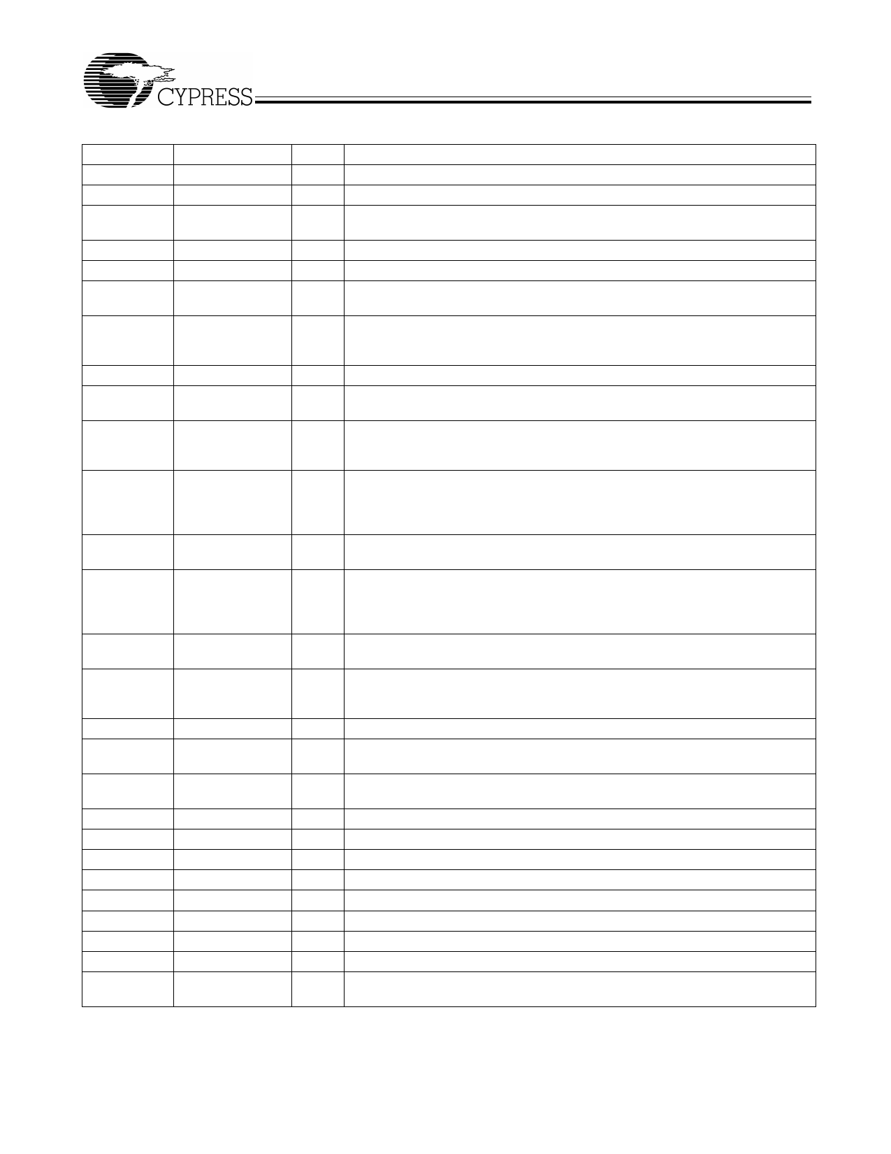
Pin Description[3]
Pin
Name
PWR
Description
1
REF
VDD 3.3V 14.318 MHz clock output
3
XIN
VDD Oscillator buffer input. Connect to a crystal or to an external clock.
4
49, 50, 52
XOUT
CPU(0:2)
VDD
Oscillator buffer output. Connect to a crystal. Do not connect when an external
clock is applied at XIN.
VDDC 2.5V Host bus clock outputs
7, 8, 9
3V66(0:2)
VDD 3.3V Fixed 66.6 MHz clock outputs
12
PCI_F
VDDP
3.3V PCI clock output. This clock continues to run when PCI_STP# is at a logic
low level.
13, 15, 16, 18,
19, 20
PCI (1:6)
3.3V PCI clock outputs. These clocks synchronously stop in a low state when
VDDP PCI_STP# is brought to a logic low level. They synchronously resume running
when PCI_STP# is brought to a logic high state.
25, 26
48M(0,1)
VDD 3.3V Fixed 48 MHz clock outputs
36
VCH_CLK
VDD
3.3V selectable 66.6 MHz or 48 MHz clock output to VCH. Spread spectrum
applies only when 66.6 MHz is selected. Select via SMBUS, byte 4 bit7.
CPU0 stop clock control input. Stops only CPU0 in a low state when asserted
34
CPU_STP#
VDD low. Using this pin to start and stop CPU0 clock insures synchronous (no short or
long clocks) transitioning of this clock.
PCI stop clock control input. When this signal is at a logic low level (0), all PCI
11
PCI_STP#
VDD
clocks (except PCI_F) stop at a logic low level. Using this pin to start and stop PCI
clocks insures synchronous (no short or long clocks) transitioning of these clocks.
This pin has no effect on the PCI_F clock.
28, 29
SEL(0,1)
VDD
3.3V LVTTL inputs for logic selection. These pins have Internal pull-ups,
typically 250k (range 200k to 800k).
30
SDATA
VDD
Serial data input pin. Conforms to the SMBUS specification of a Slave
Receive/Transmit device. This pin is an input when receiving data. It is an open
drain output when acknowledging or transmitting data. See 2-Wire SMBUS
Control Interface on page 7.
31
SCLK
VDD
Serial clock input pin. Conforms to the SMBUS specification. See 2-Wire
SMBUS Control Interface on page 7.
32
PD#
3.3V LVTTL-compatible input. When held LOW, the device enters a power down
VDD mode. This pin has an Internal Pull-Up. See Power Management Functions on
page 3.
33
TEST#
VDD 3.3V LVTTL compatible input for selecting test mode. See Table 1.
38
DCLK
VDDS
3.3V SDRAM feedback clock output. See Table 1 for frequency selection. See
Figure 4 for timing relationship.
39, 40, 42, 43,
45, 46
SDRAM(0:5)
VDDS 3.3V SDRAM clock outputs
54, 55
IOAPIC(0,1)
VDDI 2.5V IOAPIC clock outputs. See Figure 4 for timing relationships.
37, 44
VDDS
3.3V Power for SDRAM and DCLK clock output buffers
17
VDDP
3.3V Power for PCI clock output buffers
53
VDDI
2.5V Power for IOAPIC clock output buffers
51
VDDC
2.5V Power for CPU clock output buffers
2, 10, 27, 35 VDD
3.3V Common power supply
22
AVDD
Analog power
23
AVSS
Analog ground
5, 6, 14, 21, 24,
41, 47, 48, 56
VSS
Common ground pins
Note:
3. A bypass capacitor (0.1µF) should be placed as close as possible to each positive power pin. If these bypass capacitors are not close to the pins their
high-frequency filtering characteristic will be cancelled by the lead inductance of the traces.
Document #: 38-07303 Rev. **
Page 2 of 18
Share Link: