MC74HC251ADR2G(2010) Ver la hoja de datos (PDF) - ON Semiconductor
Número de pieza
componentes Descripción
Lista de partido
MC74HC251ADR2G Datasheet PDF : 9 Pages
| |||
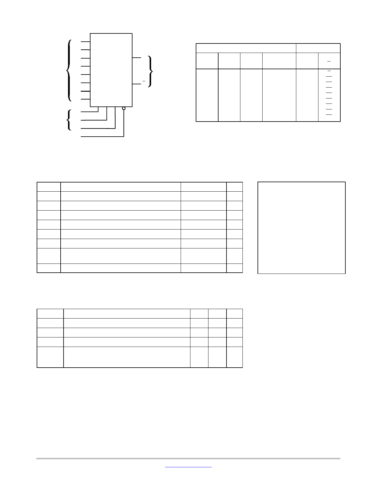
MC74HC251A
D0 4
D1 3
D2 2
5Y
DATA
INPUTS
D3 1
D4 15
D5 14
6Y
D6 13
D7 12
ADDRESS
INPUTS
A0 11
A1 10
A2 9
OUTPUT ENABLE 7
PIN 16 = VCC
PIN 8 = GND
Figure 1. Logic Diagram
DATA
OUTPUTS
FUNCTION TABLE
Inputs
Output
A2
A1
A0
Enabled
X
X
X
H
L
L
L
L
L
L
H
L
L
H
L
L
L
H
H
L
H
L
L
L
H
L
H
L
H
H
L
L
H
H
H
L
Z = high impedance
D0, D1, …, D7 = the level of the respective
D input.
Outputs
Y
Y
Z
Z
D0
D0
D1
D1
D2
D2
D3
D3
D4
D4
D5
D5
D6
D6
D7
D7
MAXIMUM RATINGS
Symbol
Parameter
Value
Unit
VCC DC Supply Voltage (Referenced to GND)
−0.5 to + 7.0
V
Vin DC Input Voltage (Referenced to GND)
−1.5 to VCC + 1.5 V
Vout DC Output Voltage (Referenced to GND)
−0.5 to VCC + 0.5 V
Iin
DC Input Current, per Pin
±25
mA
Iout DC Output Current, per Pin
±50
mA
ICC DC Supply Current, VCC and GND Pins
±75
mA
PD Power Dissipation in Still Air
SOIC Package
500
mW
TSSOP Package
TBD
Tstg Storage Temperature
−65 to + 150
°C
Stresses exceeding Maximum Ratings may damage the device. Maximum Ratings are stress
ratings only. Functional operation above the Recommended Operating Conditions is not implied.
Extended exposure to stresses above the Recommended Operating Conditions may affect device
reliability.
RECOMMENDED OPERATING CONDITIONS
Symbol
Parameter
Min
VCC DC Supply Voltage (Referenced to GND)
2.0
Vin, Vout DC Input Voltage, Output Voltage (Referenced to GND) 0
TA
Operating Temperature, All Package Types
−55
tr, tf
Input Rise and Fall Time
(Figure 2)
VCC = 2.0 V 0
VCC = 4.5 V 0
VCC = 6.0 V 0
Max Unit
6.0 V
VCC
V
+125 °C
1000 ns
500
400
This device contains protection
circuitry to guard against damage
due to high static voltages or electric
fields. However, precautions must
be taken to avoid applications of any
voltage higher than maximum rated
voltages to this high−impedance cir-
cuit. For proper operation, Vin and
Vout should be constrained to the
range GND v (Vin or Vout) v VCC.
Unused inputs must always be
tied to an appropriate logic voltage
level (e.g., either GND or VCC).
Unused outputs must be left open.
http://onsemi.com
2
Share Link: 