MC74HC251ADR2G(2010) Ver la hoja de datos (PDF) - ON Semiconductor
Número de pieza
componentes Descripción
Lista de partido
MC74HC251ADR2G Datasheet PDF : 9 Pages
| |||
MC74HC251A
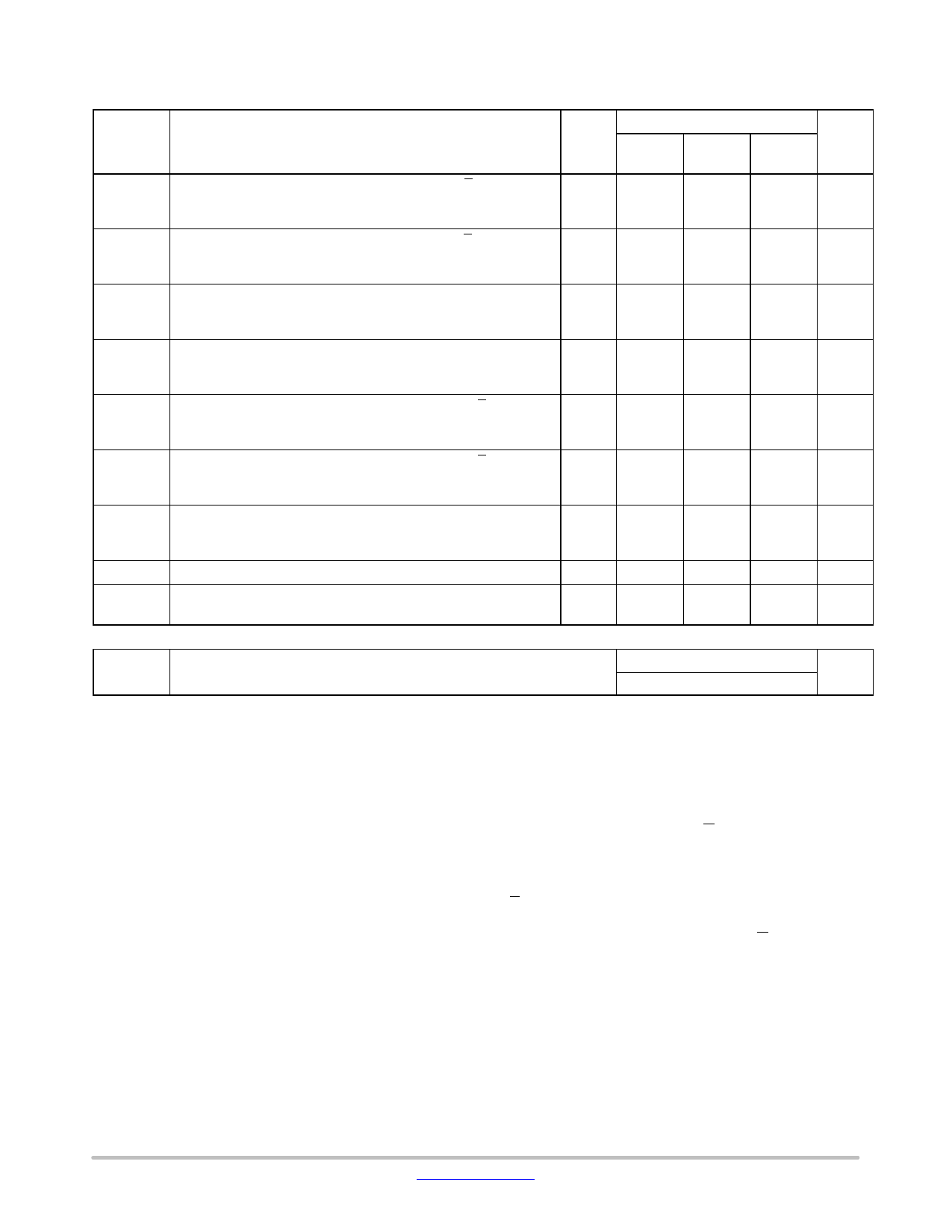
AC ELECTRICAL CHARACTERISTICS (CL = 50 pF, Input tr = tf = 6 ns)
Symbol
tPLH,
tPHL
Parameter
Maximum Propagation Delay, Input D to Output Y or Y
(Figures 2, 3 and 6)
tPLH,
tPHL
Maximum Propagation Delay, Input A to Output Y or Y
(Figures 3 and 6)
tPLZ,
tPHZ
Maximum Propagation Delay, Output Enable to Output Y
(Figures 5 and 7)
tPZL,
tPZH
Maximum Propagation Delay, Output Enable to Output Y
(Figures 5 and 7)
tPLZ,
tPHZ
Maximum Propagation Delay, Output Enable to Output Y
(Figures 5 and 7)
tPZL,
tPZH
Maximum Propagation Delay, Output Enable to Output Y
(Figures 5 and 7)
tTLH,
tTHL
Maximum Output Transition Time, Any Output
(Figures 2 and 6)
Cin
Maximum Input Capacitance
Cout
Maximum Three−State Output Capacitance
(Output in High−Impedance State)
Guaranteed Limit
VCC
− 55 to
V
25°C
v 85°C v 125°C Unit
2.0
185
230
280
ns
4.5
37
46
56
6.0
31
39
48
2.0
205
255
310
ns
4.5
41
51
62
6.0
35
43
53
2.0
195
245
295
ns
4.5
39
49
59
6.0
33
42
50
2.0
145
180
220
ns
4.5
29
36
44
6.0
25
31
38
2.0
220
275
330
ns
4.5
44
55
66
6.0
37
47
56
2.0
150
190
225
ns
4.5
30
38
45
6.0
26
33
38
2.0
75
4.5
15
6.0
13
95
110
ns
19
22
16
19
−
10
10
10
pF
−
15
15
15
pF
CPD
Power Dissipation Capacitance (Per Package)
Typical @ 25°C, VCC = 5.0 V
36
pF
PIN DESCRIPTIONS
INPUTS
D0, D1, …, D7 (Pins 4, 3, 2, 1, 15, 14, 13, 12)
Data inputs. Data on one of these eight binary inputs may
be selected to appear on the output.
CONTROL INPUTS
A0, A1, A2 (Pins 11, 10, 9)
Address inputs. The data on these pins are the binary
address of the selected input (see the Function Table).
Output Enable (Pin 7)
Output Enable. This input pin must be at a low level for
the selected data to appear at the outputs. If the Output
Enable pin is high, both the Y and Y outputs are taken to the
high−impedance state.
OUTPUTS
Y, Y (Pins 5, 6)
Data outputs. The selected data is presented at these pins
in both true (Y output) and complemented (Y output) forms.
http://onsemi.com
4
Share Link: 