AD2S1200WST Ver la hoja de datos (PDF) - Analog Devices
Número de pieza
componentes Descripción
Lista de partido
AD2S1200WST Datasheet PDF : 24 Pages
| |||
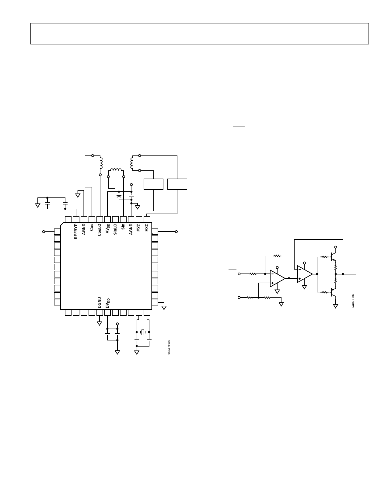
CONNECTING THE CONVERTER
Refer to Figure 5. Ground should be connected to the AGND
pin and DGND pin. Positive power supply VDD = +5 V dc ± 5%
should be connected to the AVDD pin and DVDD pin. Typical
values for the decoupling capacitors are 10 nF and 4.7 µF,
respectively. These capacitors should be placed as close to the
device pins as possible, and should be connected to both AVDD
and DVDD. If desired, the reference oscillator frequency can be
changed from the nominal value of 10 kHz using FS1 and FS2.
Typical values for the oscillator decoupling capacitors are 20 pF.
Typical values for the reference decoupling capacitors are 10 µF
and 0.01 µF, respectively.
S2
R2
10nF 10µF
R1
S6
S3
S1
4.7µF 5V
BUFFER
CIRCUIT
BUFFER
CIRCUIT
10nF
44 43 42 41 40 39 38 37 36 35 34
5V
1 DVDD
2
3
4
5
6
7
8
9
10
11
AD2S1200
33 RESET
32
31
30
29
28
27
26
25
24
DGND 23
12 13 14 15 16 17 18 19 20 21 22
5V
8.912
MHz
4.7µF
10nF
20pF
20pF
Figure 5. Connecting the AD2S1200 to a Resolver
AD2S1200
The gain of the buffer depends on the type of resolver used.
Since the specified excitation output amplitudes are matched to
the specified Sin/Cos input amplitudes, the gain of the buffer is
determined by the attenuation of the resolver.
In this recommended configuration, the converter introduces a
VREF/2 offset in the Sin, Cos signals coming from the resolver.
Of course, the SinLO and CosLO signals may be connected to a
different potential relative to ground, as long as the Sin and Cos
signals respect the recommended specifications. Note that since
the EXC/EXC outputs are differential, there is an inherent gain
of 2×.
For example, if the primary to secondary turns ratio is 2:1, the
buffer will have unity gain. Likewise, if the turns ratio is 5:1, the
gain of the buffer should be 2.5×. Figure 6 suggests a buffer
circuit. The gain of the circuit is
Gain = −(R2 / R1)
and
VOUT
= VREF
× 1+
R2
R1
−
R2
R1
×VIN
VREF is set so that VOUT is always a positive value, eliminating the
need for a negative supply.
EXC/EXC
(VIN)
R2
12V
R1
(VREF)
442Ω 1.24kΩ
5V
12V
2.7kΩ
12V
33Ω
VOUT
33Ω
2.7kΩ
Figure 6. Buffer Circuit
Separate screened twisted cable pairs are recommended for
analog inputs Sin/SinLO and Cos/CosLO. The screens should
terminate to REFOUT. To achieve the dynamic performance
specified, an 8.192 MHz crystal must be used.
Rev. 0 | Page 11 of 24
Share Link: 