TH3044.2A Ver la hoja de datos (PDF) - Melexis Microelectronic Systems
Número de pieza
componentes Descripción
Lista de partido
TH3044.2A Datasheet PDF : 12 Pages
| |||
TH3044
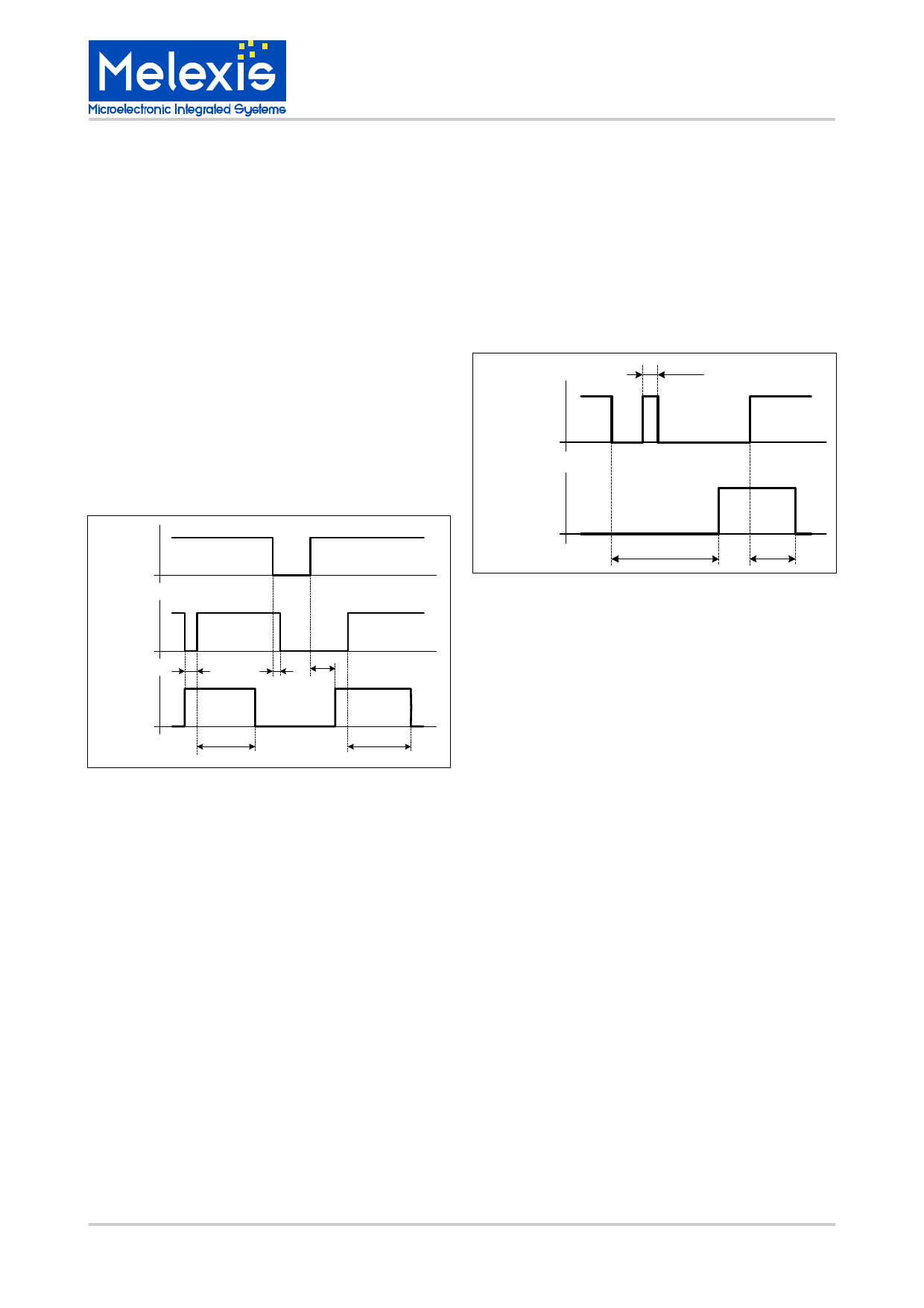
K-Bus Interface
Bit Compare
Are the signals at the pin TxD and the pin BUS
within a specified time t bc not identical, the
transmission will be interrupted.
If both signals at TxD and BUS are “High”
within the time t ena the transmission will be
enabled. To switch the TH3044 into the
receive mode a low level “0” has to be applied
to the pin Bus. If the TH3044 is part of a
complex bus system the first device which
transmits a low level “0” to the bus line forces
all other TH3044 to switch into the receive
mode. This state is valid until tena .
The bitcompare-function is frequently retrig-
gered by every new bit-comparison of two
different levels.
The bit-compare-function is activ when the pin
SEN/STA is open (not overwritten).
Constant Low
A falling edge at pin TxD (from “1” to “0”) starts
the internal constant low timer.
If the low level “0” is valid for the time t low the
transmission unit of the TH3044 will be
disabled.
The receive unit is still active. A high level “1”
at TxD with a minimum pulse width of t resets
the constant low timer.
t < trec
TxD
SEN/STA
TxD
tlow
tena
BUS
SEN/STA
t < tbc
tena
tb c
tena
Undervoltage
Undervoltage at pin VBAT or pin VCC doesn’t
occur an unwanted low level at pin Bus (see
chapter “Transmit”)
SEN/STA
The pin SEN/STA is bidirectional. Used as an
output the pin indicates whether the transmit-
path is enabled or disabled:
SEN/STA =”0”
transmission path is enabled
SEN/STA =”1”
transmission path is disabled
Using this pin as an input the transmission
path can be overwritten (independent of bit-
compare and constant-low function):
SEN/STA=”0”
forcing the transmission path free
SEN/STA=”1”
disable the transmission path
3901003044
Rev. 003
Page 6
Nov/02
Share Link: 