LTC1480 Ver la hoja de datos (PDF) - Linear Technology
Número de pieza
componentes Descripción
Lista de partido
LTC1480 Datasheet PDF : 8 Pages
| |||
LTC1480
ABSOLUTE AXI U RATI GS
(Note 1)
Supply Voltage (VCC) ................................................ 7V
Control Input Voltage ..................... – 0.3V to VCC + 0.3V
Driver Input Voltage ....................... – 0.3V to VCC + 0.3V
Driver Output Voltage ........................................... ±14V
Receiver Input Voltage .......................................... ±14V
Receiver Output Voltage ................ – 0.3V to VCC + 0.3V
Operating Temperature Range
LTC1480C ....................................... 0°C ≤ TA ≤ 70°C
LTC1480I .................................... – 40°C ≤ TA ≤ 85°C
Storage Temperature Range ................. – 65°C to 150°C
Lead Temperature (Soldering, 10 sec).................. 300°C
UW U
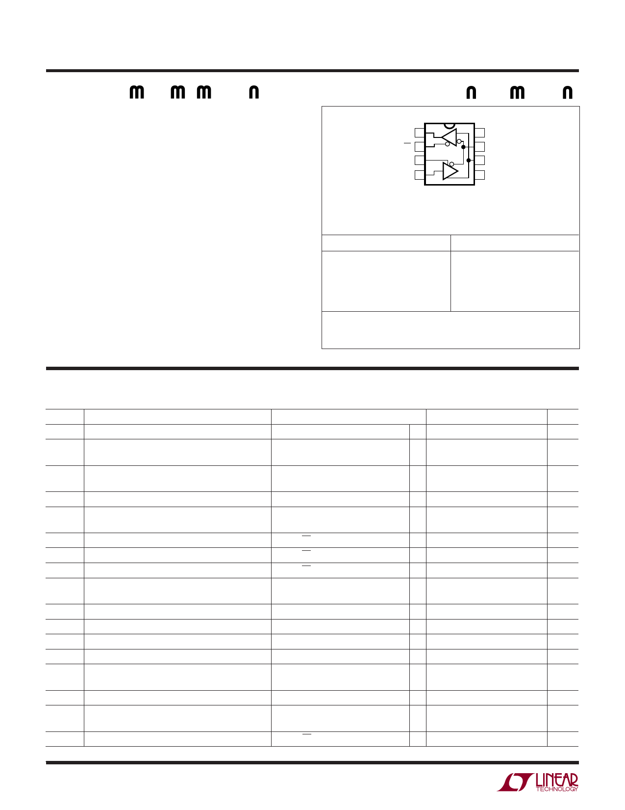
PACKAGE/ORDER I FOR ATIO
TOP VIEW
RO 1
RE 2
R
8 VCC
7B
DE 3
DI 4
D
6A
5 GND
N8 PACKAGE
8-LEAD PDIP
S8 PACKAGE
8-LEAD PLASTIC SO
TJMAX = 125°C, θJA = 130°C/ W (N8)
TJMAX = 125°C, θJA = 150°C/ W (S8)
ORDER PART NUMBER S8 PART MARKING
LTC1480CN8
LTC1480IN8
LTC1480CS8
LTC1480IS8
1480
1480I
Order Options Tape and Reel: Add #TR
Lead Free: Add #PBF Lead Free Tape and Reel: Add #TRPBF
Lead Free Part Marking: http://www.linear.com/leadfree/
Consult LTC Marketing for parts specified with wider operating temperature ranges.
ELECTRICAL CHARACTERISTICS The ● denotes the specifications which apply over the full operating
temperature range. VCC = 3.3V (Notes 2, 3).
SYMBOL PARAMETER
CONDITIONS
MIN
TYP
MAX UNITS
VOD1
Differential Driver Output Voltage (Unloaded)
VOD2
Differential Driver Output Voltage (with Load)
IO = 0V
R = 27Ω (RS485) (Figure 1)
R = 50Ω (RS422)
●
● 1.5
● 2.0
3.3
V
3.3
V
V
∆VOD
Change in Magnitude of Driver Differential Output R = 27Ω or R = 50Ω (Figure 1)
●
Voltage for Complementary Output States
0.2
V
VOC
Driver Common Mode Output Voltage
R = 27Ω or R = 50Ω (Figure 1)
●
∆⏐VOC⏐ Change in Magnitude of Driver Common Mode
R = 27Ω or R = 50Ω (Figure 1)
●
Output Voltage for Complementary Output States
2
V
0.2
V
VIH
Input HIGH Voltage
DE, DI, RE
●2
V
VIL
Input LOW Voltage
DE, DI, RE
●
0.8
V
IIN1
Input Current
DE, DI, RE
●
±2
µA
IIN2
Input Current (A, B)
DE = 0, VCC = 0V or 3.6V, VIN = 12V ●
DE = 0, VCC = 0V or 3.6V, VIN = – 7V ●
1.0
mA
– 0.8
mA
VTH
Differential Input Threshold Voltage for Receiver – 7V ≤ VCM ≤ 12V
● – 0.2
0.2
V
∆VTH
Receiver Input Hysteresis
VCM = 0V
70
mV
VOH
Receiver Output HIGH Voltage
IO = – 4mA, VID = 200mV
●2
V
VOL
Receiver Output LOW Voltage
IO = 4mA, VID = – 200mV
●
0.4
V
IOZR
Three-State (High Impedance) Output
Current at Receiver
VCC = Max, 0.4V ≤ VO ≤ 2.4V
●
±1
µA
RIN
Receiver Input Resistance
ICC
Supply Current
– 7V ≤ VCM ≤ 12V
No Load, Output Enabled
No Load, Output Disabled
● 12
kΩ
●
400
600
µA
●
300
500
µA
ISHDN
Supply Current in Shutdown Mode
DE = 0, RE = VCC
1
10
µA
1480fa
2
Share Link: 