LTC1480 Ver la hoja de datos (PDF) - Linear Technology
Número de pieza
componentes Descripción
Lista de partido
LTC1480 Datasheet PDF : 8 Pages
| |||
LTC1480
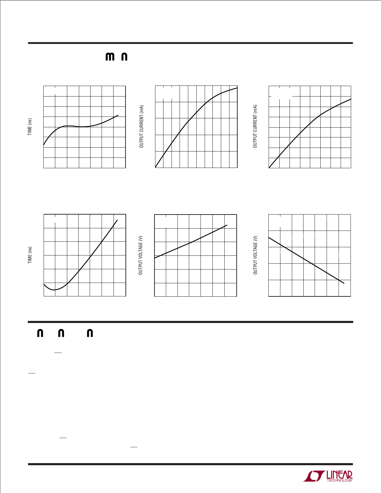
TYPICAL PERFORMANCE CHARACTERISTICS
Driver Skew vs Temperature
7.0
VCC = 3.3V
6.5
6.0
5.5
5.0
4.5
4.0
3.5
3.0
– 40 – 20
0 20 40 60
TEMPERATURE (°C)
80 100
1480 G04
Receiver Output Low Voltage
vs Output Current
25
VCC = 3.3V
TA = 25°C
20
15
10
5
0
0 0.2 0.4 0.6 0.8 1.0 1.2 1.4 1.6 1.8 2.0
OUTPUT VOLTAGE (V)
1480 G05
Receiver ⏐tPLH – tPHL⏐
vs Temperature
12
VCC = 3.3V
10
Receiver Output Low Voltage
vs Temperature
0.6
VCC = 3.3V
IO = 8mA
0.5
8
0.4
6
0.3
4
0.2
2
0.1
Receiver Output High Voltage
vs Output Current
– 16
VCC = 3.3V
– 14 TA = 25°C
– 12
– 10
–8
–6
–4
–2
0
3.30 3.05 2.80 2.55 2.30 2.05 1.80 1.55 1.30
OUTPUT VOLTAGE (V)
1480 G06
Receiver Output High Voltage
vs Temperature
3.0
VCC = 3.3V
IO = 8mA
2.8
2.6
2.4
2.2
0
–40 –20
0 20 40 60
TEMPERATURE (°C)
UU U
PI FU CTIO S
80 100
1480 G07
0
–40 –20
0 20 40 60
TEMPERATURE (°C)
80 100
1480 G08
2.0
– 40 – 20
0 20 40 60
TEMPERATURE (°C)
80 100
1480 G09
RO (Pin 1): Receiver Output. If the receiver output is
enabled (RE LOW) and A > B by 200mV, then RO will be
HIGH. If A < B by 200mV, then RO will be LOW.
RE (Pin 2): Receiver Output Enable. A LOW enables the
receiver output, RO. A HIGH input forces the receiver
output into a high impedance state.
DE (Pin 3): Driver Outputs Enable. A HIGH on DE enables
the driver output. A, B and the chip will function as a line
driver. A low input will force the driver outputs into a high
impedance state and the chip will function as a line
receiver. If RE is high and DE is LOW, the part will enter a
low power (1µA) shutdown state. If RE is low and DE is
high, the driver outputs will be fed back to the receiver and
the receive output will correspond to the driver input.
DI (Pin 4): Driver Input. If the driver outputs are enabled
(DE HIGH) then a low on DI forces the outputs A LOW and
B HIGH. A HIGH on DI with the driver outputs enabled will
force A HIGH and B LOW.
GND (Pin 5): Ground.
A (Pin 6): Driver Output/Receiver Input.
B (Pin 7): Driver Output/Receiver Input.
VCC (Pin 8): Positive Supply. 3.0V < VCC < 3.6V.
1480fa
4
Share Link: 