LT1581CT7 Ver la hoja de datos (PDF) - Linear Technology
Número de pieza
componentes Descripción
Lista de partido
LT1581CT7 Datasheet PDF : 12 Pages
| |||
LT1581/LT1581-2.5
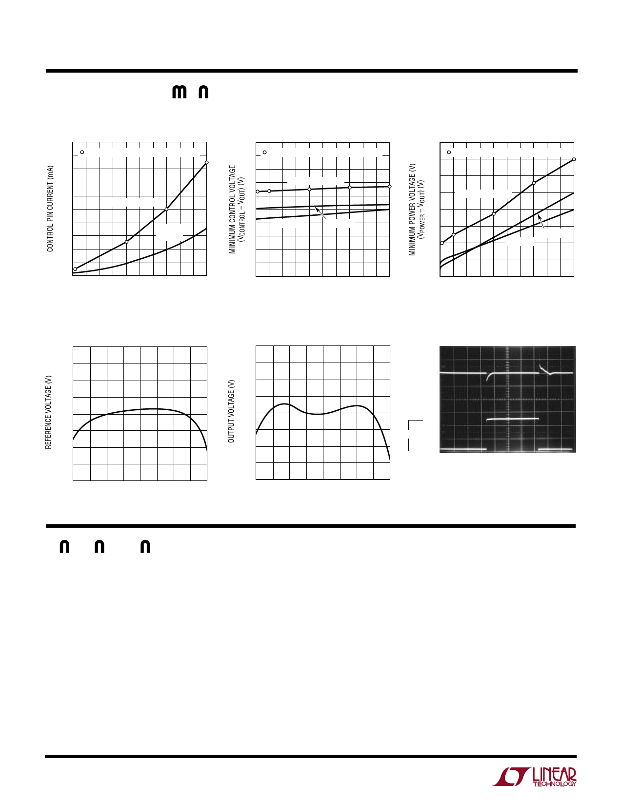
TYPICAL PERFORMANCE CHARACTERISTICS
Control Pin Current vs
Output Current
200
180 INDICATES GUARANTEED TEST POINTS
160
140
120
DATA SHEET LIMIT
100
80
TYPICAL
60
DEVICE
40
20
0
0 1 2 3 4 5 6 7 8 9 10
OUTPUT CURRENT (A)
1581 G01
LT1581 Reference Voltage vs
Temperature
1.262
1.259
1.256
1.253
1.250
1.247
1.244
1.241
1.238
–50 –25
0 25 50 75 100 125 150
TEMPERATURE (°C)
1581 G04
Dropout Voltage —
Minimum Control Voltage
2
INDICATES GUARANTEED TEST POINTS
Dropout Voltage —
Minimum Power Voltage
0.8
INDICATES GUARANTEED TEST POINTS
0.7
DATA SHEET LIMIT
1
TJ = 125°C
TJ = 25°C
0.6
0.5
DATA SHEET LIMIT
0.4
0.3
TJ = 125°C
0.2
TJ = 25°C
0.1
0
0 1 2 3 4 5 6 7 8 9 10
OUTPUT CURRENT (A)
1581 G02
0
0 1 2 3 4 5 6 7 8 9 10
OUTPUT CURRENT (A)
1581 G03
LT1581-2.5 Output Voltage vs
Temperature
2.512
Load Current Step Response
2.509
2.506
VOUT
50mV/DIV
2.503
2.500
2.497
2.494
2.491
10A
LOAD
400mA
50µs/DIV
1581 G06
2.488
–50 –25
0 25 50 75 100 125 150
TEMPERATURE (°C)
1581 G05
PIN FUNCTIONS
ADJUST (Pin 1): This pin is the negative side of the
reference voltage for the device. Transient response can
be improved by adding a small bypass capacitor from the
ADJUST pin to ground. For fixed voltage devices the
ADJUST pin is also brought out to allow the user to add a
bypass capacitor.
GND (Pin 2, Fixed Voltage Devices Only): For fixed
voltage devices this is the bottom of the resistor divider
that sets the output voltage.
SENSE (Pin 3): This pin is the positive side of the reference
voltage for the device. With this pin it is possible to Kelvin
sense the output voltage at the load.
OUTPUT (Pin 4): This is the power output of the device.
VPOWER (Pin 5): This is the collector to the power device
of the LT1581. The output load current is supplied through
this pin. For the device to regulate, the voltage at this pin
must be between 0.1V and 0.7V greater than the output
voltage (see Dropout specifications).
VCONTROL (Pin 6): This pin is the supply pin for the control
circuitry of the device. The current flow into this pin will
be about 1% of the output current. For the device to
regulate, the voltage at this pin must be between 1.0V and
1.35V greater than the output voltage (see Dropout
specifications).
4
Share Link: 