LT1581CT7 Ver la hoja de datos (PDF) - Linear Technology
Número de pieza
componentes Descripción
Lista de partido
LT1581CT7 Datasheet PDF : 12 Pages
| |||
LT1581/LT1581-2.5
APPLICATIONS INFORMATION
network must handle until the regulator throttles to the
load current level. Capacitors are not ideal elements and
contain parasitic resistance and inductance. These para-
sitic elements dominate the change in output voltage at
the beginning of a transient load step change. The ESR of
the output capacitors produces an instantaneous step in
output voltage (∆V = ∆I)(ESR). The ESL of the output
capacitors produces a droop proportional to the rate of
change of the output current (V = L)(∆I/∆t). The output
capacitance produces a change in output voltage
proportional to the time until the regulator can respond
(∆V = ∆t)(∆I/C). These transient effects are illustrated in
Figure 4 .
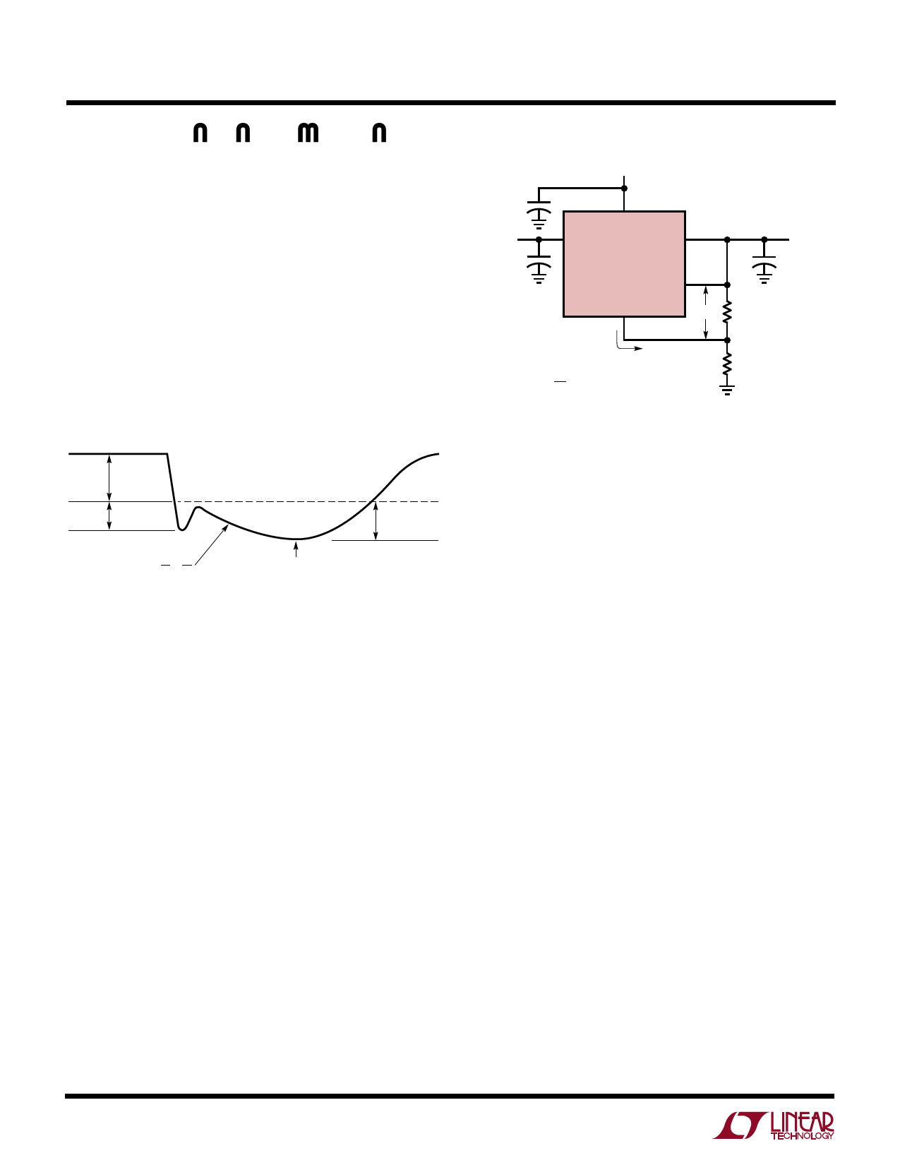
+
VPOWER +
VCONTROL
CONTROL
POWER
OUTPUT
LT1581
SENSE
ADJ
VREF
+
R1
VOUT
IADJ = 60µA
( ) VOUT = VREF
1 + R2
R1
+ IADJ (R2)
R2
1581 F05
Figure 5. Setting Output Voltage
ESR
EFFECTS
ESL
EFFECTS
SLOPE,
V
t
=
∆I
C
POINT AT WHICH REGULATOR
TAKES CONTROL
CAPACITANCE
EFFECTS
1581 F04
Figure 4
minimum load current of 10mA. The current out of the
ADJUST pin adds to the current from R1. The ADJUST pin
current is small, typically 60µA. The output voltage contri-
bution of the ADJUST pin current is small and only needs
to be considered when very precise output voltage setting
is required. Note that the top of the resistor divider should
be connected directly to the SENSE pin for best regulation.
See the section on grounding and Kelvin sensing above.
The use of capacitors with low ESR, low ESL and good
high frequency characteristics is critical in meeting the
output voltage tolerances of these high speed micropro-
cessors. These requirements dictate a combination of
high quality, surface mount, tantalum and ceramic capaci-
tors. The location of the decoupling network is critical to
transient performance. Place the decoupling network as
close to the processor pins as possible because trace runs
from the decoupling capacitors to the processor pins are
inductive. The ideal location for the decoupling network is
actually inside the microprocessor socket cavity. In addi-
tion, use large power and ground plane areas to minimize
distribution drops.
Output Voltage
The adjustable version of the LT1581 develops a 1.25V
reference voltage between the SENSE pin and the ADJUST
pin (see Figure 5). Placing a resistor R1 between these two
terminals causes a constant current to flow through R1
and down through R2 to set the overall output voltage.
Normally, R1 is chosen so that this current is the specified
Protection Diodes
In normal operation the LT1581 does not require protec-
tion diodes. Older 3-terminal regulators require protection
diodes between the OUTPUT pin and the INPUT pin or
between the ADJUST pin and the OUTPUT pin to prevent
die overstress.
On the LT1581, internal resistors limit internal current
paths on the ADJUST pin. Therefore even with bypass
capacitors on the ADJUST pin, no protection diode is
needed to ensure device safety under short-circuit con-
ditions. The ADJUST pin can be driven on a transient
basis ±7V with respect to the output without any device
degradation.
A protection diode between the OUTPUT pin and the
VPOWER pin is usually not needed. An internal diode
between the OUTPUT pin and the VPOWER pin on the
LT1581 can handle microsecond surge currents of 50A to
100A. Even with large value output capacitors it is difficult
to obtain those values of surge currents in normal opera-
tion. Only with large values of output capacitance, such as
8
Share Link: 