RTL8100 Ver la hoja de datos (PDF) - Realtek Semiconductor
Número de pieza
componentes Descripción
Lista de partido
RTL8100 Datasheet PDF : 58 Pages
| |||
RTL8100B(L)
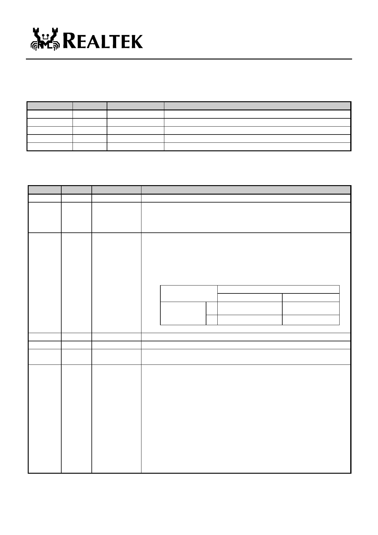
5.10 CONFIG 0: Configuration Register 0
(Offset 0051h, R/W)
Bit
R/W
Symbol
Description
7
R
SCR
Scrambler Mode: Always 0.
6
R
PCS
PCS Mode: Always 0.
5
R
T10
10 Mbps Mode: Always 0.
4-3
R
PL1, PL0
Select 10 Mbps medium type: Always (PL1, PL0) = (1, 0)
2-0
-
-
Reserved
5.11 CONFIG 1: Configuration Register 1
(Offset 0052h, R/W)
Bit
R/W
Symbol
Description
7-6
R/W
LEDS1-0 Refer to the LED PIN definition. The initial value of these bits comes from the 93C46.
5
R/W
DVRLOAD Driver Load: Software may use this bit to make sure that the driver has been
loaded. Writing 1 is 1. Writing 0 is 0. When the command register bits IOEN,
MEMEN, and BMEN of the PCI configuration space are written, the
RTL8100B(L) will clear this bit automatically.
4
R/W
LWACT LWAKE active mode: The LWACT bit and LWPTN bit in CONFIG4 register
are used to program the LWAKE pin’s output signal. According to the
combination of these two bits, there may be 4 choices of LWAKE signal, i.e.,
active high, active low, positive (high) pulse, and negative (low) pulse. The
output pulse width is about 150 ms.
The default value of each of these two bits is 0, i.e., the default output signal of
LWAKE pin is an active high signal.
LWAKE output
LWACT
0
1
0
Active high*
Active low
LWPTN
1
Positive pulse
Negative pulse
* Default value.
3
R
MEMMAP Memory Mapping: The operational registers are mapped into PCI memory space.
2
R
IOMAP
I/O Mapping: The operational registers are mapped into PCI I/O space.
1
R/W
VPD
Set to enable Vital Product Data: The VPD data is stored in 93C46 from within
offset 40h-7Fh.
0
R/W
PMEn
Power Management Enable:
Writable only when 93C46CR register EEM1=EEM0=1
Let A denote the New_Cap bit (bit 4 of the Status Register) in the PCI
Configuration space offset 06H.
Let B denote the Cap_Ptr register in the PCI Configuration space offset 34H.
Let C denote the Cap_ID (power management) register in the PCI Configuration
space offset 50H.
Let D denote the power management registers in the PCI Configuration space
offset from 52H to 57H.
Let E denote the Next_Ptr (power management) register in the PCI
Configuration space offset 51H.
PMEn Description
1 A=1, B=50h, C=01h, D valid, E=0
0 A=B=C=E=0, D not valid
2001-11-9
20
Rev.1.41
Share Link: 