LM25115 Ver la hoja de datos (PDF) - National ->Texas Instruments
Número de pieza
componentes Descripción
Lista de partido
LM25115 Datasheet PDF : 17 Pages
| |||
Synchronization (SYNC) and Feed-forward (RAMP) (Continued)
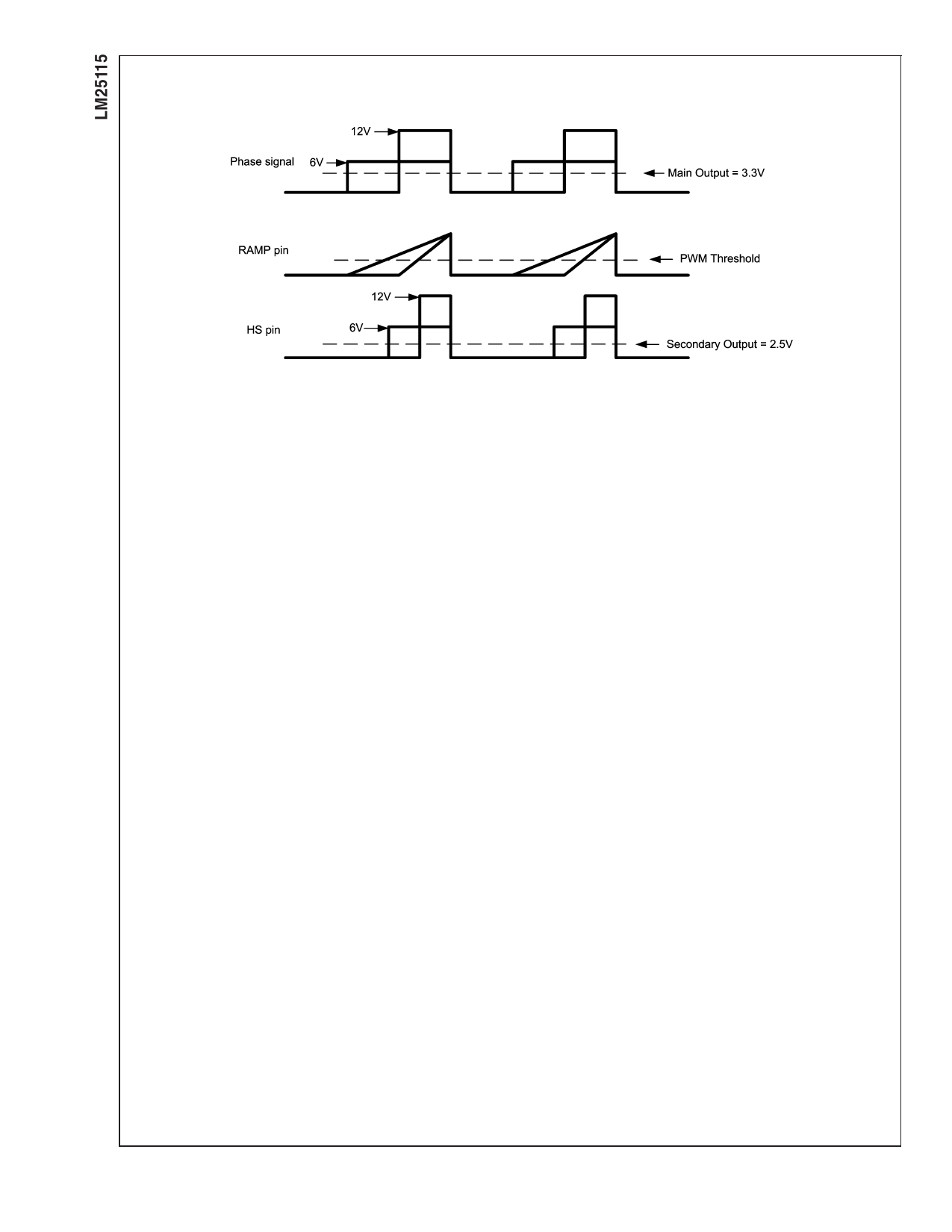
FIGURE 3. Line Feed-forward Waveforms
20172613
The recommended SYNC input current range is 50µA to
150µA. The SYNC pin resistor (RSYNC) should be selected to
set the SYNC current (ISYNC) to 150µA with the maximum
phase signal amplitude, VPHASE(max). This will guarantee
that ISYNC stays within the recommended range over a 3:1
change in phase signal amplitude. The SYNC pin resistor is
therefore:
RSYNC = (VPHASE(max) / 150µA) - 2.5kΩ
Once ISYNC has been established by selecting RSYNC, the
RAMP signal amplitude may be programmed by selecting
the proper RAMP pin capacitor value. The recommended
peak amplitude of the RAMP waveform is 1V to 1.75V. The
CRAMP capacitor is chosen to provide the desired RAMP
amplitude with the nominal phase signal voltage and pulse
width.
Where
CRAMP = (3 x ISYNC x TON ) / VRAMP
CRAMP = RAMP pin capacitance
ISYNC = SYNC pin current current
TON = corresponding phase signal pulse width
VRAMP = desired RAMP amplitude (1V to 1.75V)
For example,
Main channel output = 3.3V. Phase signal maximum ampli-
tude = 12V. Phase signal frequency = 250kHz
• Set ISYNC = 150µA with phase signal at maximum ampli-
tude (12V):
ISYNC = 150µA = VPHASE(max) / (RSYNC + 2.5 kΩ) = 12V /
(RSYNC + 2.5 kΩ)
RSYNC = 12V/150µA - 2.5kΩ = 77.5kΩ
• TON = Main channel duty cycle / Phase frequency =
(3.3V/12V) / 250kHz = 1.1µs
• Assume desired VRAMP = 1.5V
• CRAMP = (3 x ISYNC x TON ) / VRAMP = (3 x 150µA x 1.1µs)
/ 1.5V
• CRAMP = 330pF
Error Amplifier and Soft-Start (FB,
CO, & COMP, SS)
An internal wide bandwidth error amplifier is provided within
the LM25115 for voltage feedback to the PWM controller.
The amplifier’s inverting input is connected to the FB pin.
The output of the auxiliary converter is regulated by connect-
ing a voltage setting resistor divider between the output and
the FB pin. Loop compensation networks are connected
between the FB pin and the error amplifier output (COMP).
The amplifier’s non-inverting input is internally connected to
the SS pin. The SS pin is biased at 0.75V by a resistor
divider connected to the internal 1.27V bandgap reference.
When the VCC voltage is below the UVLO threshold, the SS
pin is discharged to ground. When VCC rises and exceeds
the positive going UVLO threshold (4.25V), the SS pin is
released and allowed to rise. If an external capacitor is
connected to the SS pin, it will be charged by the internal
resistor divider to gradually increase the non-inverting input
of the error amplifier to 0.75V. The equivalent impedance of
the SS resistor divider is nominally 60kΩ which determines
the charging time constant of the SS capacitor. During start-
up, the output of the LM25115 converter will follow the
exponential equation:
VOUT(t) = VOUT(final) x (1 - exp(-t/RSS x CSS))
Where
Rss = internal resistance of SS pin (60kΩ)
Css = external Soft-Start capacitor
VOUT(final) = regulator output set point
The initial ∆v / ∆t of the output voltage is VOUT(final) / Rss x
Css and VOUT will be within 1% of the final regulation level
after 4.6 time constants or when t = 4.6 x Rss x Css.
Pull-up current for the error amplifier output is provided by an
internal 300µA current source. The PWM threshold signal at
the COMP pin can be controlled by either the open drain
error amplifier or the open drain current amplifier connected
through the CO pin to COMP. Since the internal error ampli-
fier is configured as an open drain output it can be disabled
by connecting FB to ground. The current sense amplifier and
current limiting function will be described in a later section.
www.national.com
10
Share Link: 