LM25115 Ver la hoja de datos (PDF) - National ->Texas Instruments
Número de pieza
componentes Descripción
Lista de partido
LM25115 Datasheet PDF : 17 Pages
| |||
Detailed Operating Description
The LM25115 controller contains all of the features neces-
sary to implement multiple output power converters utilizing
the Secondary Side Post Regulation (SSPR) technique. The
SSPR technique develops a highly efficient and well regu-
lated auxiliary output from the secondary side switching
waveform of an isolated power converter. Regulation of the
auxiliary output voltage is achieved by leading edge pulse
width modulation (PWM) of the main channel duty cycle.
Leading edge modulation is compatible with either current
mode or voltage mode control of the main output. The
LM25115 drives external high side and low side NMOS
power switches configured as a synchronous buck regulator.
A current sense amplifier provides overload protection and
operates over a wide common mode input range from 0V to
13.5V. Additional features include a low dropout (LDO) bias
regulator, error amplifier, precision reference, adaptive dead
time control of the gate driver signals and thermal shutdown.
A programmable oscillator provides a PWM clock signal
when the LM25115 is powered by a dc input (free-run mode)
instead of the phase signal of the main channel converter
(SSPR mode).
Low Drop-out Bias Regulator
(VCC)
The LM25115 contains an internal LDO regulator that oper-
ates over an input supply range from 4.5V to 30V. The output
of the regulator at the VCC pin is nominally regulated at 7V
and is internally current limited to 40mA. VCC is the main
supply to the internal logic, PWM controller, and gate driver
circuits. When power is applied to the VBIAS pin, the regu-
lator is enabled and sources current into an external capaci-
tor connected to the VCC pin. The recommended output
capacitor range for the VCC regulator is 0.1uF to 100uF.
When the voltage at the VCC pin reaches the VCC under-
voltage lockout threshold of 4.25V, the controller is enabled.
The controller is disabled if VCC falls below 4.0V (250mV
hysteresis). In applications where an appropriate regulated
dc bias supply is available, the LM25115 controller can be
powered directly through the VCC pin instead of the VBIAS
pin. In this configuration, it is recommended that the VCC
and the VBIAS pins be connected together such that the
external bias voltage is applied to both pins. The allowable
VCC range when biased from an external supply is 4.5V to
7V.
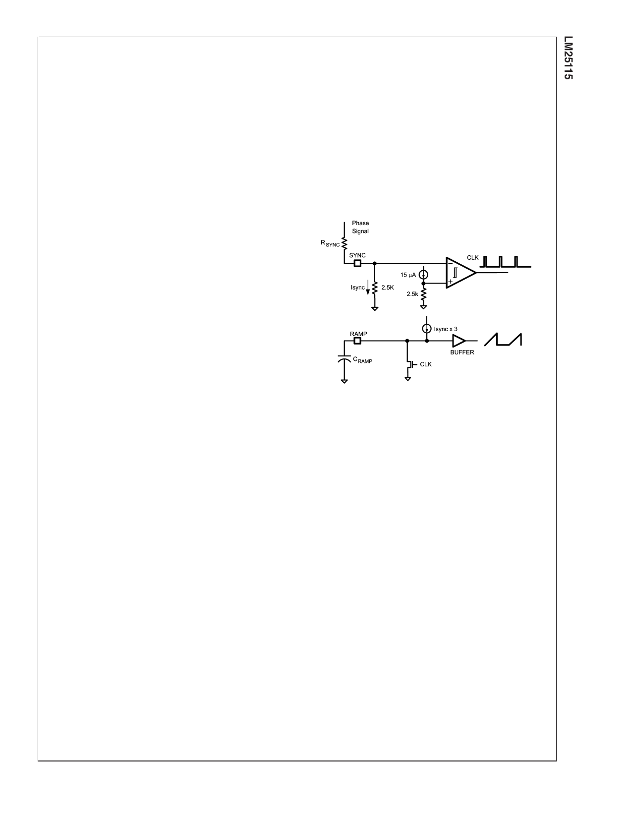
Synchronization (SYNC) and
Feed-forward (RAMP)
The pulsing “phase signal” from the main converter synchro-
nizes the PWM ramp and gate drive outputs of the LM25115.
The phase signal is the square wave output from the trans-
former secondary winding before rectification (Figure 1). A
resistor connected from the phase signal to the low imped-
ance SYNC pin produces a square wave current (ISYNC) as
shown in Figure 2. A current comparator at the SYNC input
monitors ISYNC relative to an internal 15µA reference. When
ISYNC exceeds 15µA, the internal clock signal (CLK) is reset
and the capacitor connected to the RAMP begins to charge.
The current source that charges the RAMP capacitor is
equal to 3 times the ISYNC current. The falling edge of the
phase signal sets the CLK signal and discharges the RAMP
capacitor until the next rising edge of the phase signal. The
RAMP capacitor is discharged to ground by a low imped-
ance (100Ω) n-channel MOSFET. The input impedance at
SYNC pin is 2.5kΩ which is normally much less than the
external SYNC pin resistance.
20172612
FIGURE 2. Line Feed-forward Diagram
The RAMP and SYNC functions illustrated in Figure 2 pro-
vide line voltage feed-forward to improve the regulation of
the auxiliary output when the input voltage of the main
converter changes. Varying the input voltage to the main
converter produces proportional variations in amplitude of
the phase signal. The main channel PWM controller adjusts
the pulse width of the phase signal to maintain constant
volt*seconds and a regulated main output as shown in Fig-
ure 3. The variation of the phase signal amplitude and dura-
tion are reflected in the slope and duty cycle of the RAMP
signal of the LM25115 (ISYNC α phase signal amplitude). As
a result, the duty cycle of the LM25115 is automatically
adjusted to regulate the auxiliary output voltage with virtually
no change in the PWM threshold voltage. Transient line
regulation is improved because the PWM duty cycle of the
auxiliary converter is immediately corrected, independent of
the delays of the voltage regulation loop.
9
www.national.com
Share Link: 