RF2483PCBA Ver la hoja de datos (PDF) - RF Micro Devices
Número de pieza
componentes Descripción
Lista de partido
RF2483PCBA Datasheet PDF : 28 Pages
| |||
RF2483
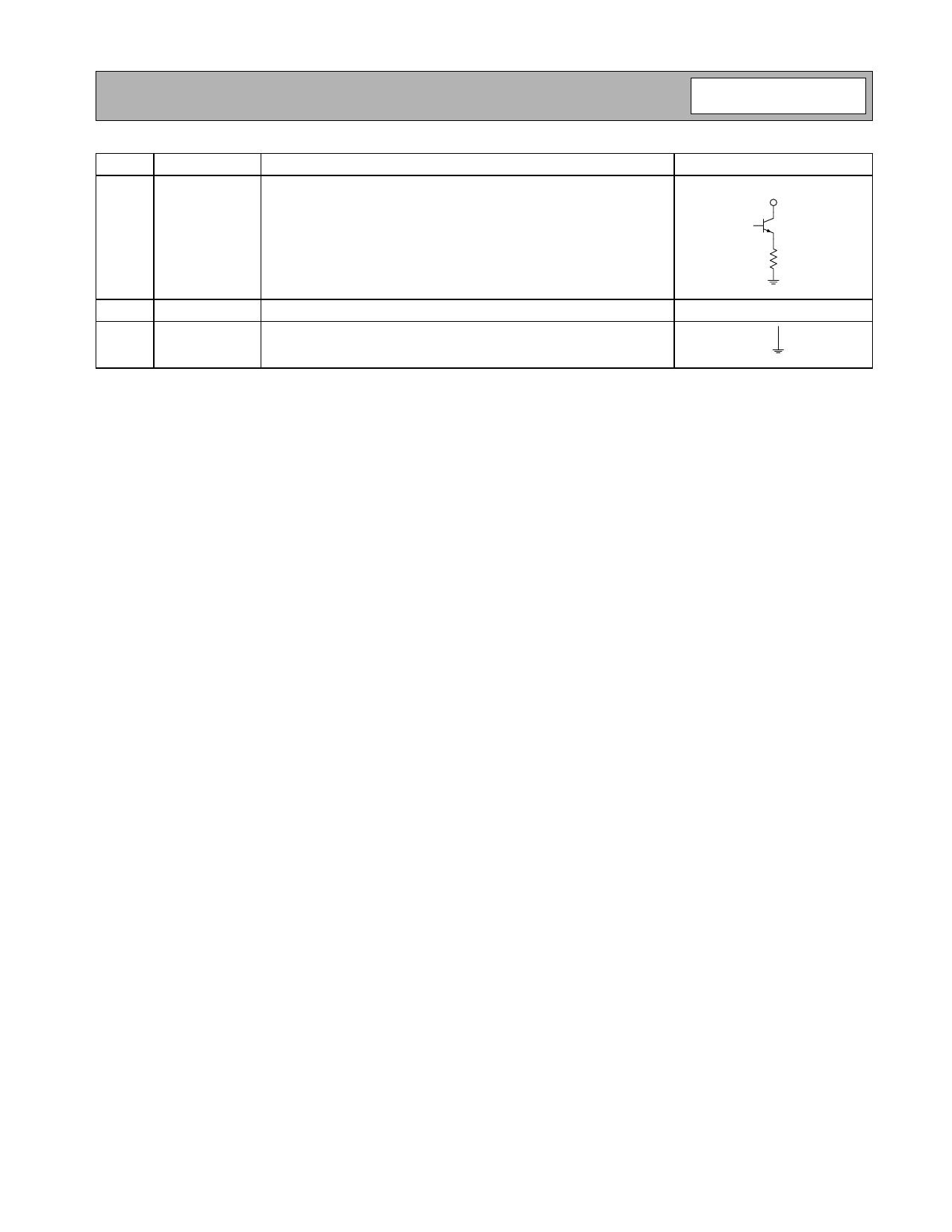
Pin
19
20
Die
Flag
Function
RF OUT HB
GND3
GND4
Description
RF high band output. Open collector output.
The output should be biased at VCC through an inductor that can be
used to form part of an output matching circuit.
In our proposed applications circuit some power is dissipated in R4
(180Ω) which appears as a de-Qing resistor in parallel with the output
inductor L3. If R4 is eliminated and the RFOUT HB pin is re-matched to
50Ω it is possible to get approximately 3dB extra power out of the
device in high band mode.
Ground for RF output sections.
Ground for modulator, variable gain amplifier and substrate.
Interface Schematic
Rev A8 060203
5-41
Share Link: 