RF2483PCBA Ver la hoja de datos (PDF) - RF Micro Devices
Número de pieza
componentes Descripción
Lista de partido
RF2483PCBA Datasheet PDF : 28 Pages
| |||
RF2483
Application Notes
The baseband inputs must be driven with balanced differential signals. We suggest amplitude and phase matching
<0.5dB and <0.5°. Phase or gain imbalances between the complementary input signals will cause additional distortion
including some second order baseband distortion.
The common-mode voltage on the baseband inputs should be well controlled at 1.2V. We suggest that the common-
mode DC voltage be 1.2V+0.05V. The common-mode DC voltage is used to bias the modulator; hence, deviations from
1.2V will result in changes in the current consumption, noise and intermodulation performance.
The chip is designed to be driven with a single-ended LO signal.
The GC DEC and VREF output pins should be decoupled to ground. We recommend a 10nF capacitor on VREF, and a
1nF capacitor on GC DEC. The purpose of this capacitor is to filter out low frequency noise (20MHz) in the gain control
lines, which may cause noise on the RF signal. The capacitor on the GC DEC line will effect the settling time response to
a change in power control voltage. A 1nF capacitor equates to around a 200ns settling time, and a 0.5nF capacitor
equates to a 100ns settling time. There is a trade-off between settling time and phase noise as you start to apply gain
control.
The ground lines for the LO sections, GNDLO and GND1, are brought out of the chip independently from the ground to
the RF and modulator sections. This isolates the LO signals from the RF output sections.
The GND LO pin is effectively the complementary LO input for both the high band and low band LO signals. It has signif-
icant amounts of LO signal flowing through it. This is brought out as an independent ground to try to enable the PCB
board designer to isolate the LO return from the RF output sections and general chip ground.
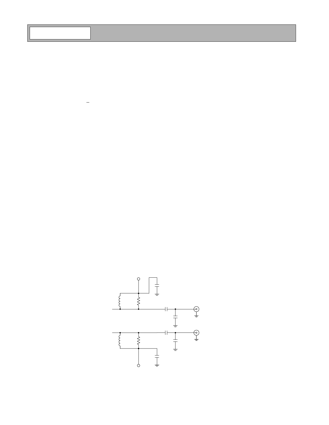
The RF output ports of the RF2483 consist of open collector architecture and require pull up inductors to the supply volt-
age. This, in conjunction with a DC blocking capacitor provides a simple, broadband L-match network as shown in the
schematic diagram. A shunt resistor is included to control the Q of the matching network and set the modulator output
power. In this case, both outputs were designed to provide 0dBm.
An alternate output match containing a third harmonic trap was evaluated. This circuit uses a tapped-C matching net-
work, whereby the shunt C provides a low impedance path near the third harmonic frequency. Although an additional
component is required, the benefit of suppressing the third harmonic distortion may improve overall system intermodula-
tion. This network has been shown to provide better than 20dB of improved suppression in high-band mode.
VCC
C4
100 pF
L3
2.2 nH
R4
180 Ω
L4
10 nH
R6
130 Ω
C11
2 pF
C15
6 pF
C12
1 pF
C13
2 pF
J4
RFOUT HB
J8
RFOUT LB
C6
100 pF
VCC
Figure 1. Alternate RF output match with third-harmonic suppression.
5-42
Rev A8 060203
Share Link: 