RF2483PCBA Ver la hoja de datos (PDF) - RF Micro Devices
Número de pieza
componentes Descripción
Lista de partido
RF2483PCBA Datasheet PDF : 28 Pages
| |||
RF2483
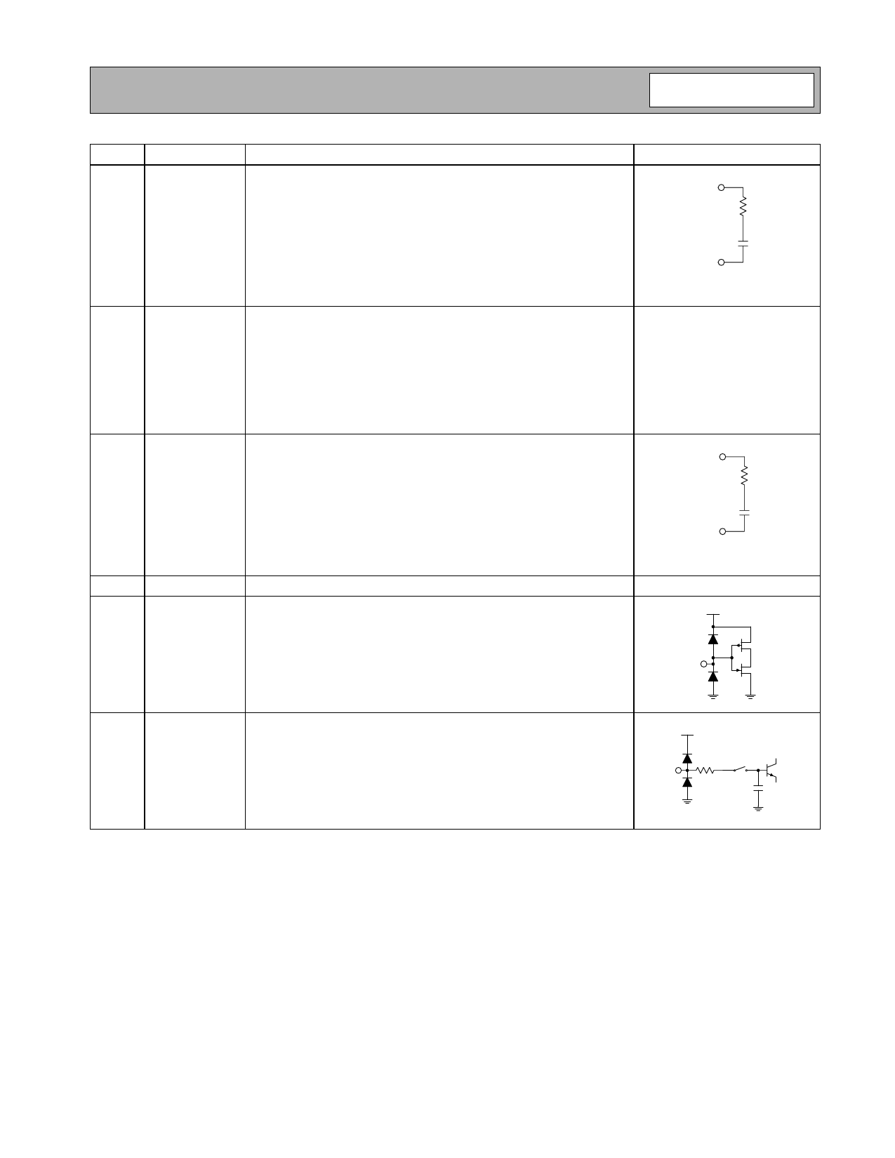
Pin
7
8
9
10
11
Function
LOLB
GND LO
LOHB
GND1
BAND SEL
Description
Interface Schematic
Local oscillator input low band.
This input is biased internally at around 1.6V when the chip is in low
band mode and 0V when the chip is in high band mode or powered
down. The LO signal typically needs to be AC coupled.
The noise performance, carrier suppression at low output powers and
sideband suppression are all a function of LO power.
The optimum LO power is between 0dBm and 3dBm.
The device will work with LO powers as low as -20dBm however this is
at the expense of higher noise performance at high output powers and
poorer sideband suppression.
Ground return for the local oscillator input signals.
The GND LO pin is effectively the complementary LO input for both the
high band and low band LO signals. It has significant amounts of LO
signal flowing through it. This pin is brought out as an independent
ground to enable the PCB board designer to isolate the LO return from
the RF outputs ground and the general chip ground.
It is recommended that this ground is kept isolated from the die flag
ground. Any connections between the GND LO and any other ground
should be made through a ground plane.
Local oscillator input high band.
This input is biased internally at around 1.6V when the chip is in high
band mode and 0V when the chip is in low band mode or powered
down. The LO HB signal typically needs to be AC coupled.
The noise performance, carrier suppression at low output powers and
sideband suppression are all a function of LO power.
The optimum LO power is between 0dBm and 3dBm.
The device will work with LO powers as low as -20dBm however this is
at the expense of higher noise performance at high output powers and
poorer sideband suppression.
Ground for LO buffers.
LOLB
GNDLO
See pins 7 and 9.
LOHB
GND LO
See pin 6.
Band select input to define active mode.
VCC2
CMOS input.
Logic 1 (1.4V to VCC)=High band mode.
Logic 2 (0V to 0.5V)=Low band mode.
12
QSIG N Quadrature channel negative baseband input port. See QSIGP.
VCC2
50 Ω
12 pF
Rev A8 060203
5-39
Share Link: 