FM24CL16B Ver la hoja de datos (PDF) - Cypress Semiconductor
Número de pieza
componentes Descripción
Lista de partido
FM24CL16B Datasheet PDF : 14 Pages
| |||
AC Test Conditions
Input Pulse Levels
Input rise and fall times
Input and output timing levels
0.1 VDD to 0.9 VDD
10 ns
0.5 VDD
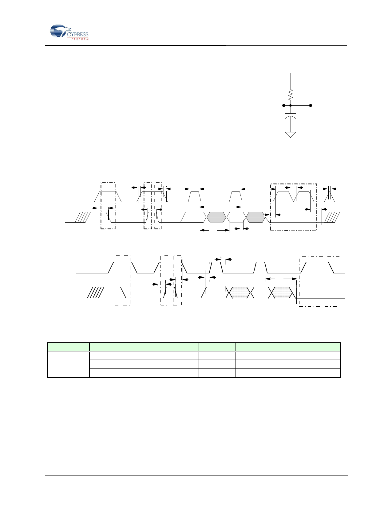
Diagram Notes
All start and stop timing parameters apply to both read and write cycles.
Clock specifications are identical for read and write cycles. Write timing
parameters apply to slave address, word address, and write data bits.
Functional relationships are illustrated in the relevant data sheet
sections. These diagrams illustrate the timing parameters only.
FM24CL16B - 16Kb 3V I2C F-RAM
Equivalent AC Load Circuit
3.6V
Output
1100
100 pF
Read Bus Timing
SCL
SDA
t SU:STA
Start
Write Bus Timing
SCL
SDA
tR
tBUF
t HIGH
` tF
Stop Start
1/fSCL
tAA
tLOW
t DH
t SU:STO
t HD:STA
t HD:DAT
t SU:DAT
Start
Stop Start
tSP
t SP
t HD:DAT
t SU:DAT
Acknowledge
t AA
Acknowledge
Data Retention
Symbol
Parameter
TDR
@ +85ºC
@ +80ºC
@ +75ºC
Min
Max
Units
Notes
10
-
Years
19
-
Years
38
-
Years
Document Number: 001-84456 Rev. *A
Page 10 of 14
Share Link: 