FM24CL16B Ver la hoja de datos (PDF) - Cypress Semiconductor
Número de pieza
componentes Descripción
Lista de partido
FM24CL16B Datasheet PDF : 14 Pages
| |||
FM24CL16B - 16Kb 3V I2C F-RAM
AC Parameters (TA = -40 C to + 85 C, VDD =2.7V to 3.65V unless otherwise specified)
Symbol Parameter
Min Max Min Max Min Max
fSCL
tLOW
tHIGH
tAA
SCL Clock Frequency
Clock Low Period
Clock High Period
SCL Low to SDA Data Out Valid
0 100 0 400 0 1000
4.7
1.3
0.6
4.0
0.6
0.4
3
0.9
0.55
Units
kHz
s
s
s
tBUF
Bus Free Before New Transmission 4.7
1.3
0.5
s
tHD:STA Start Condition Hold Time
4.0
0.6
0.25
s
tSU:STA Start Condition Setup for Repeated 4.7
0.6
0.25
s
Start
tHD:DAT
tSU:DAT
tR
Data In Hold Time
Data In Setup Time
Input Rise Time
0
0
0
ns
250
100
100
ns
1000
300
300 ns
tF
tSU:STO
Input Fall Time
Stop Condition Setup
300
300
100 ns
4.0
0.6
0.25
s
tDH
Data Output Hold
0
0
0
ns
(from SCL @ VIL)
tSP
Noise Suppression Time Constant
50
50
50 ns
on SCL, SDA
Notes : All SCL specifications as well as start and stop conditions apply to both read and write operations.
1 The speed-related specifications are guaranteed characteristic points from DC to 1 MHz.
2 This parameter is periodically sampled and not 100% tested.
Notes
1
2
2
Capacitance (TA = 25 C, f=1.0 MHz, VDD = 3V)
Symbol
Parameter
Max
CI/O
Input/Output Capacitance (SDA)
8
CIN
Input Capacitance
6
Units
pF
pF
Notes
1 This parameter is periodically sampled and not 100% tested.
Notes
1
1
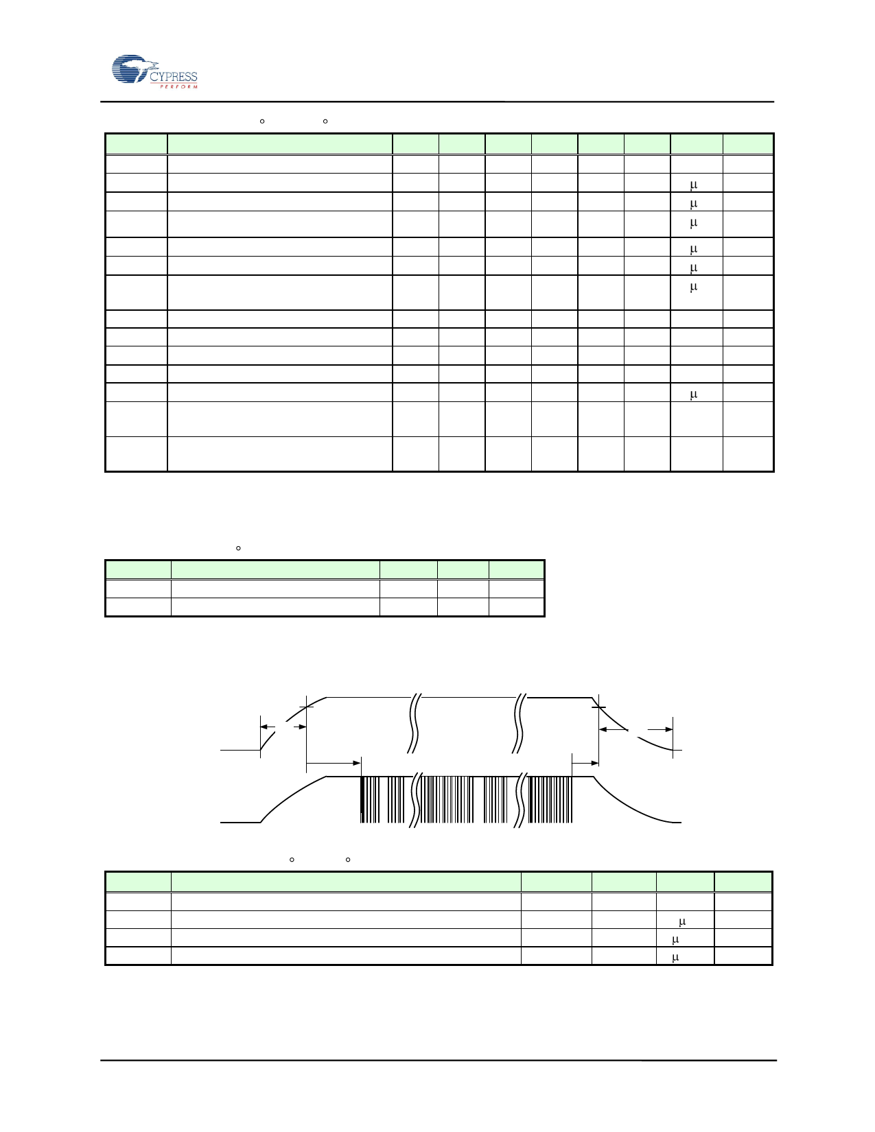
Power Cycle Timing
VDD
VDD min.
tVR
tPU
tVF
tPD
SDA,SCL
Power Cycle Timing (TA = -40 C to +85 C, VDD = 2.7V to 3.65V unless otherwise specified)
Symbol Parameter
Min
Max
tPU
Power Up (VDD min) to First Access (Start condition)
1
-
tPD
Last Access (Stop condition) to Power Down (VDD min)
0
-
tVR
VDD Rise Time
30
-
tVF
VDD Fall Time
30
-
Notes
1. Slope measured at any point on VDD waveform.
Units
ms
s
s/V
s/V
Notes
1
1
Document Number: 001-84456 Rev. *A
Page 9 of 14
Share Link: 