IRF720 Ver la hoja de datos (PDF) - New Jersey Semiconductor
Número de pieza
componentes Descripción
Lista de partido
IRF720 Datasheet PDF : 3 Pages
| |||
IRF720, IRF721, IRF722, IRF723 Devices
Source-Drain Diode Ratings and Characteristics
Parameter
Type Mm. Typ, Max. Units
Test Conditions
Ic
Continuous Source Current
(Body Diodel
ALL
-
-
3.3
A Modified MOSFET symbol showing the integre)
Reverse p-n junction icctifier.
-~-—3t
ISM Pulsed Source Current
(Body Diodel (D
AU ~
~
13
A
Vsp
t,,
OpR
ton
Diode Forward Vfaltage ®
Reverse Recovery Time
Reverse Recovery Charge
Forward Turn-On Time
ALL
-
-
1.6
V Tj = 25°C, ls = 3.3A. VGS = 0V
ALL 120
270 600
ns Tj - 2S°C, IF - 3.3A. <i\Ul = 100 A/,a
ALL 0.64 1.4 3.0
fC
ALL Intrinsic turn-on time is negligible. Turn-on speed is substantially controlled by LS t LQ.
Thermal Resistance
RtnJC JuncUon-to-Csse
RlhCS Case-to-SInk
RthjA Junction-to-Ambient
ALL -
-
2.5 K/W®
ALL
-
0.50
- IOW® Mounting surface fiat, smooth, and greased
ALL
-
-
30 K W ® Typical socket mount
Typical SPICE Computer Model Parameters (ForMore Information SeeApplication Note AN-975)
Device
Level.
SPICE
MOSFET
Model
W(m),
Channel
Width
Llpm),
Channel
Length
Theta (1M,
Mobility
Modulation
UO (CM2/V-S),
Surface
Mobility
VTOCV),
Threshold
Voltage
R1 (D),
Drain
Resistance
R2(Q),
Source
Resistance
RG ID).
Gate
Resistance
ALL
3
0.279
1.2
0.30
450
4.00
1.4
0.02
1.5
CGSO (pfl.
Gate-
Source
Capacitance
770
CGD(F)
Gate-
Drain
Capacitance
ca
E1 (V),
Voltage Dependent
Voltage Source
2 + 0.995 VDQ
LO InH),
Drain
Inductance
4.5
LS(nH),
Source
Inductance
7.6
LGInH),
Gate
Inductance
7.6
HIM,
Diode
Saturation
Current
3.6 x 10'13
C8 = 1500 pf + 1.8 x 10⁻²² (VQt;)48
0> Repetitive Rating; Pulse width limited by
maximum function temperature (see figure 5)
Refer to current HEXFET reliability report
® 0 VDD • BOV. Starting Tj - 26°C,
L - 31 mH.RQ = 250,
Peak IL - 3.3A.
01 ISD s 3.3A, d/dt £ 66A/M3,
VOD =i 8VDSS, Tj i 160°C
Suggested RQ - 180
® Pulse width s 300 ia; Duty Cycle s 2%
K/W = °C/W
W/K - W/°C
RSIO),
Diode
Bulk
Resistance
0.026
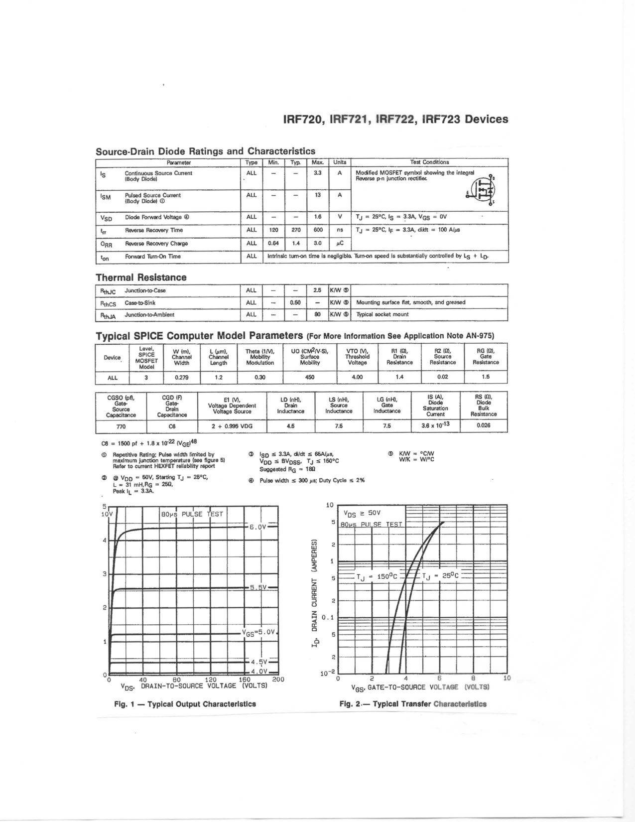
80HS PULSE TEST
6.0V—i
V6S=5.0VJ
•4.5V-
A nv
0
40
80
ISO
160
200
VDS. DRAIN-TO-SQUHCE VOLTAGE (VOLTS)
Fig. 1 — Typical Output Characteristics
Vnc z E 0V
•^ 80pl. PUL si- ESJ
j/ ^
s
a
/( [
/y T , = isc °c
J'\1i4/ r i - 250(
0.1
/'/'g/ /i// =
10-2
I
1i j
)
t
i
t
1(
Vss. GATE-TO-SOURCE VOLTAGE (VOLTS)
Fig. 2— Typical Transfer Characteristics
Share Link: 