FCPF11N60F_13 Ver la hoja de datos (PDF) - Fairchild Semiconductor
Número de pieza
componentes Descripción
Lista de partido
FCPF11N60F_13 Datasheet PDF : 10 Pages
| |||
Package Marking and Ordering Information
Device Marking
FCPF11N60F
Device
FCPF11N60F
Package
TO-220F
Reel Size
-
Tape Width
-
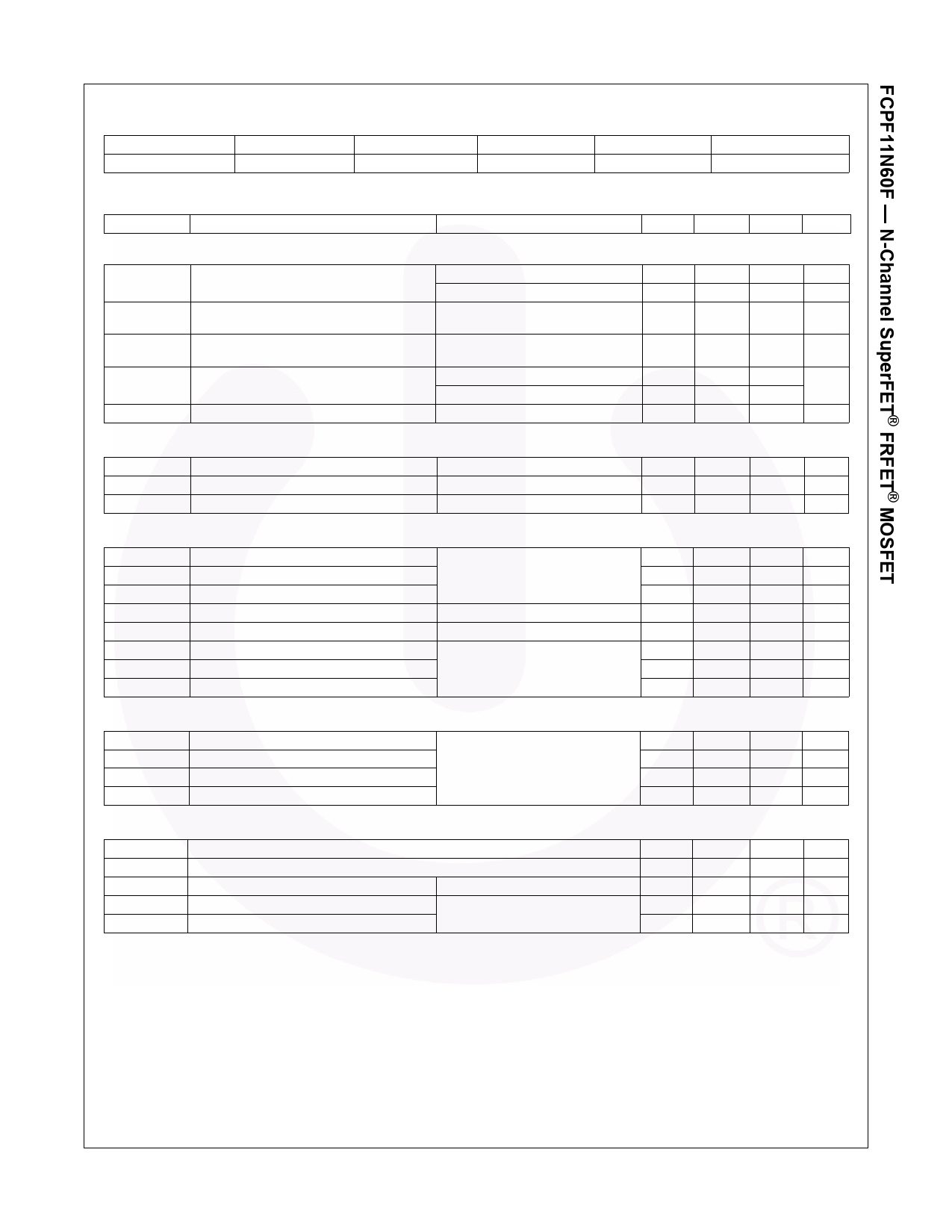
Electrical Characteristics TC = 25oC unless otherwise noted
Symbol
Parameter
Test Conditions
Off Characteristics
BVDSS
ΔBVDSS
/ ΔTJ
BVDS
IDSS
IGSS
Drain to Source Breakdown Voltage
Breakdown Voltage Temperature
Coefficient
Drain-Source Avalanche Breakdown
Voltage
Zero Gate Voltage Drain Current
Gate to Body Leakage Current
VGS = 0 V, ID = 250 μA, TC = 25oC
VGS = 0 V, ID = 250 μA, TC = 150oC
ID = 250 μA, Referenced to 25oC
VGS = 0 V, ID = 11 A
VDS = 600 V, VGS = 0 V
VDS = 480 V, TC = 125oC
VGS = ±30 V, VDS = 0 V
On Characteristics
VGS(th)
RDS(on)
gFS
Gate Threshold Voltage
Static Drain to Source On Resistance
Forward Transconductance
VGS = VDS, ID = 250 μA
VGS = 10 V, ID = 5.5 A
VDS = 40 V, ID = 5.5 A
Dynamic Characteristics
Ciss
Coss
Crss
Coss
Coss(eff.)
Qg(tot)
Qgs
Qgd
Input Capacitance
Output Capacitance
Reverse Transfer Capacitance
Output Capacitance
Effective Output Capacitance
Total Gate Charge at 10V
Gate to Source Gate Charge
Gate to Drain “Miller” Charge
VDS = 25 V, VGS = 0 V,
f = 1.0 MHz
VDS = 480 V, VGS = 0 V, f = 1.0 MHz
VDS = 0 V to 400 V, VGS = 0 V
VDS = 480 V, ID = 11 A,
VGS = 10 V
(Note 4)
Switching Characteristics
td(on)
tr
td(off)
tf
Turn-On Delay Time
Turn-On Rise Time
Turn-Off Delay Time
Turn-Off Fall Time
VDD = 300 V, ID = 11 A,
RG = 25 Ω
(Note 4)
Drain-Source Diode Characteristics
IS
Maximum Continuous Drain to Source Diode Forward Current
ISM
Maximum Pulsed Drain to Source Diode Forward Current
VSD
Drain to Source Diode Forward Voltage
VGS = 0 V, ISD = 11 A
trr
Reverse Recovery Time
Qrr
Reverse Recovery Charge
VdIGFS/d=t =01V0,0ISAD/μ=s11 A,
Notes:
1. Repetitive rating: pulse-width limited by maximum junction temperature.
2. IAS = 5.5 A, VDD = 50 V, RG = 25 Ω, starting TJ = 25°C.
3. ISD ≤ 11 A, di/dt ≤ 200 A/μs, VDD ≤ BVDSS, starting TJ = 25°C.
4. Essentially independent of operating temperature.
Min.
600
-
-
-
-
-
-
3.0
-
-
-
-
-
-
-
-
-
-
-
-
-
-
-
-
-
-
-
Quantity
50
Typ. Max. Unit
-
-
V
650
-
V
0.6
-
V/oC
700
-
V
-
-
1
10
μA
-
±100 nA
-
5.0
V
0.32
0.38
Ω
6
-
S
1148 1490 pF
671
870
pF
63
82
pF
35
-
pF
95
-
pF
40
52
nC
7.2
-
nC
21
-
nC
34
80
ns
98
205
ns
119
250
ns
56
120
ns
-
11
A
-
33
A
-
1.4
V
120
-
ns
0.8
-
μC
©2008 Fairchild Semiconductor Corporation
2
FCPF11N60F Rev. C1
www.fairchildsemi.com
Share Link: 