AD8351ARM_04 Ver la hoja de datos (PDF) - Analog Devices
Número de pieza
componentes Descripción
Lista de partido
AD8351ARM_04 Datasheet PDF : 16 Pages
| |||
AD8351
ABSOLUTE MAXIMUM RATINGS*
Supply Voltage VPOS . . . . . . . . . . . . . . . . . . . . . . . . . . . . . 6 V
PWUP Voltage . . . . . . . . . . . . . . . . . . . . . . . . . . . . . . . VPOS
Internal Power Dissipation . . . . . . . . . . . . . . . . . . . . . 320 mW
JA . . . . . . . . . . . . . . . . . . . . . . . . . . . . . . . . . . . . . . . 125°C/W
Maximum Junction Temperature . . . . . . . . . . . . . . . . . 125°C
Operating Temperature Range . . . . . . . . . . . . –40°C to +85°C
Storage Temperature Range . . . . . . . . . . . . . –65°C to +150°C
Lead Temperature Range (Soldering 60 sec) . . . . . . . . . 300°C
*Stresses above those listed under Absolute Maximum Ratings may cause perma-
nent damage to the device. This is a stress rating only; functional operation of the
device at these or any other conditions above those indicated in the operational
section of this specification is not implied. Exposure to absolute maximum rating
conditions for extended periods may affect device reliability.
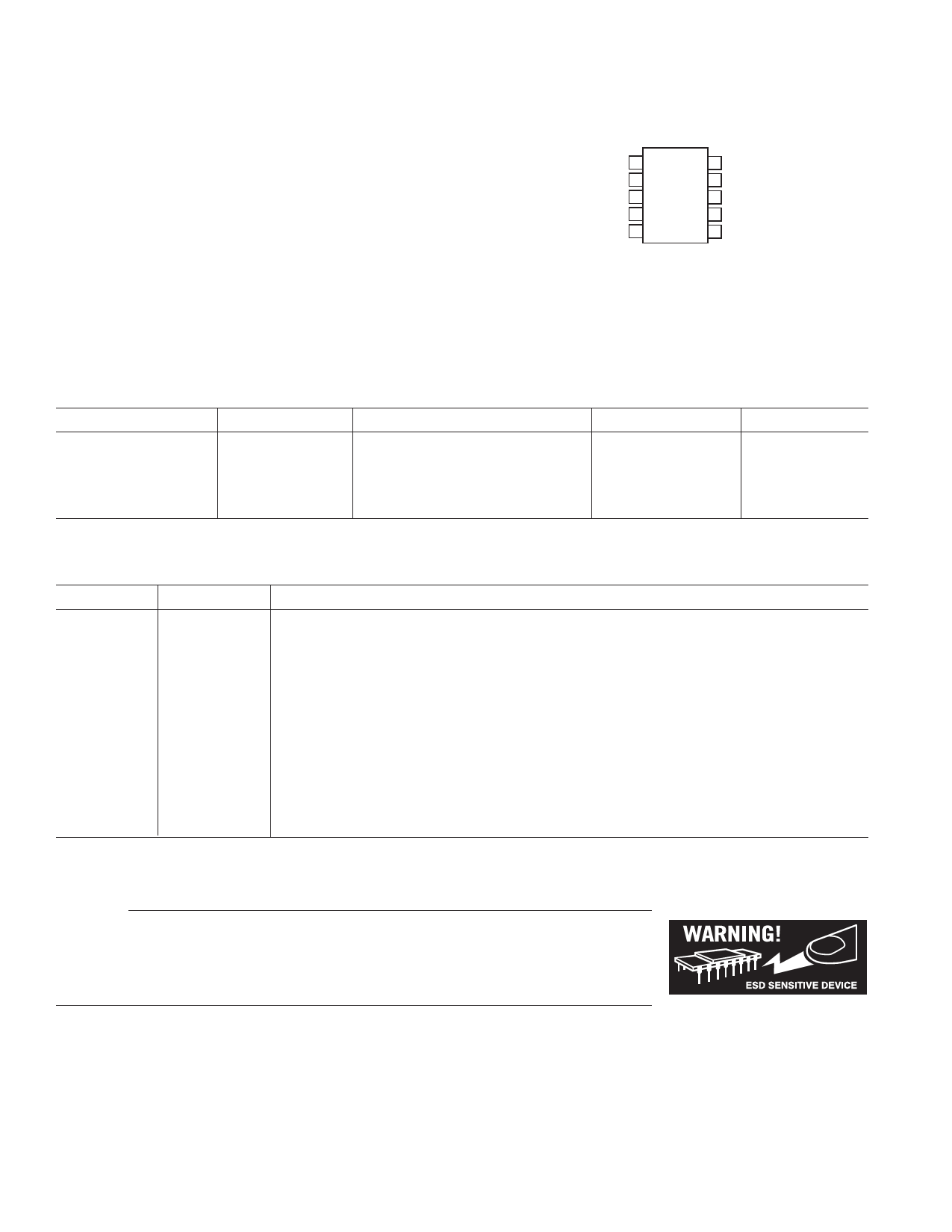
PIN CONFIGURATION
PWUP 1
10 VOCM
RGP1 2 AD8351 9 VPOS
INHI 3 TOP VIEW 8 OPHI
INLO 4 (Not to Scale) 7 OPLO
RGP2 5
6 COMM
Model
AD8351ARM
AD8351ARM-R2
AD8351ARM-REEL7
AD8351-EVAL
Temp. Range
–40°C to +85°C
–40°C to +85°C
–40°C to +85°C
ORDERING GUIDE
Package Description
10-Lead MSOP, 7" Tape and Reel
10-Lead MSOP, 7" Tape and Reel
10-Lead MSOP, 7" Tape and Reel
Evaluation Board
Package Option
RM-10
RM-10
RM-10
Branding
JDA
JDA
JDA
Pin No.
1
2
3
4
5
6
7
8
9
10
Name
PWUP
RGP1
INHI
INLO
RGP2
COMM
OPLO
OPHI
VPOS
VOCM
PIN FUNCTION DESCRIPTIONS
Function
Apply a positive voltage (1.3 V ≤ VPWUP ≤ VPOS ) to activate device.
Gain Resistor Input 1.
Balanced Differential Input. Biased to midsupply, typically ac-coupled
Balanced Differential Input. Biased to midsupply, typically ac-coupled.
Gain Resistor Input 2.
Device Common. Connect to low impedance ground.
Balanced Differential Output. Biased to VOCM, typically ac-coupled.
Balanced Differential Output. Biased to VOCM, typically ac-coupled.
Positive Supply Voltage. 3 V to 5.5 V.
Voltage applied to this pin sets the common-mode voltage at both the input and output.
Typically decoupled to ground with a 0.1 µF capacitor.
CAUTION
ESD (electrostatic discharge) sensitive device. Electrostatic charges as high as 4000 V readily
accumulate on the human body and test equipment and can discharge without detection. Although the
AD8351 features proprietary ESD protection circuitry, permanent damage may occur on devices
subjected to high energy electrostatic discharges. Therefore, proper ESD precautions are recommended
to avoid performance degradation or loss of functionality.
–4–
REV. B
Share Link: 