AD8351ARM_04 Ver la hoja de datos (PDF) - Analog Devices
Número de pieza
componentes Descripción
Lista de partido
AD8351ARM_04 Datasheet PDF : 16 Pages
| |||
50
7
25
100
6
AD8351
10
200
500
50⍀
SERIES L
150⍀
0
500
200
SHUNT C
100
50
25
10
5
4
RL = 1000⍀
3
RL = 500⍀
2
RL = 150⍀
1
0
0
100
1000
RG (⍀)
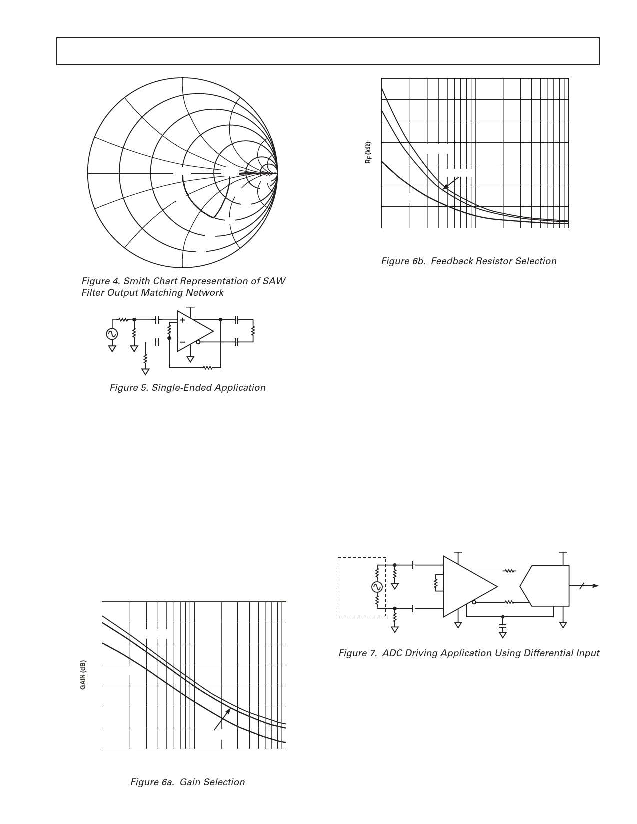
Figure 6b. Feedback Resistor Selection
Figure 4. Smith Chart Representation of SAW
Filter Output Matching Network
50⍀
0.1F
50⍀ RG
AD8351
0.1F
0.1F RL
0.1F
25⍀
RF
Figure 5. Single-Ended Application
SINGLE-ENDED-TO-DIFFERENTIAL OPERATION
The AD8351 can easily be configured as a single-ended-to-
differential gain block, as illustrated in Figure 5. The input signal
is ac-coupled and applied to the INHI input. The unused input is
ac-coupled to ground. The values of C1 through C4 should be
selected such that their reactances are negligible at the desired
frequency of operation. To balance the outputs, an external feed-
back resistor, RF, is required. To select the gain resistor and the
feedback resistor, refer to Figures 6a and 6b. From Figure 6a,
select an RG for the required dB gain at a given load. Next, select
from Figure 6b an RF resistor for the selected RG and load.
Even though the differential balance is not perfect under these
conditions, the distortion performance is still impressive. TPCs 10
and 11 show the second and third harmonic distortion perfor-
mance when driving the input of the AD8351 using a single-ended
50 Ω source.
35
30
RL = 1000⍀
25
20
RL = 150⍀
15
10
5
RL = 500⍀
0
0
100
1000
RG (⍀)
ADC DRIVING
The circuit in Figure 7 represents a simplified front end of the
AD8351 driving the AD6645, which is a 14-bit, 105 MSPS A/D
converter. For optimum performance, the AD6645 and the
AD8351 are driven differentially. The resistors R1 and R2 present
a 50 Ω differential input impedance to the source with R3 and R4
providing isolation from the A/D input. The gain setting resistor
for the AD8351 is RG. The AD6645 presents a 1 kΩ differential
load to the AD8351 and requires a 2.2 V p-p differential signal
between AIN and AIN for a full-scale output. This AD8351
circuit then provides the gain, isolation, and source matching for
the AD6645. The AD8351 also provides a balanced input, not
provided by the balun, to the AD6645, which is essential for
second-order cancellation. The signal generator is bipolar,
centered around ground. Connecting the VOCM pin (10) of the
AD8351 to the VREF pin of the AD6645 sets the common-mode
output voltage of the AD8351 at 2.4 V. This voltage is bypassed
with a 0.1 µF capacitor. Increasing the gain of the AD8351 will
increase the system noise and thus decrease the SNR but will
not significantly affect the distortion. The circuit in Figure 7 can
provide SFDR performance of better than –90 dBc with a 10 MHz
input and –80 dBc with a 70 MHz input at a gain of 10 dB.
BALANCE
50⍀
SOURCE
100nF INHI
25⍀
RG
100nF INLO
25⍀
OPHI
25⍀
AD8351
OPLO 25⍀
VOCM
AIN
AD6645
AIN VREF
DIGITAL
OUT
Figure 7. ADC Driving Application Using Differential Input
The circuit of Figure 8 represents a single-ended input to differ-
ential output configuration of the AD8351 driving the AD6645.
In this case, R1 provides the input impedance. RG is the gain
setting resistor. The resistor RF is required to balance the output
voltages required for second-order cancellation by the AD6645
and can be selected using a chart. (See the Single-Ended-to-
Differential Operation section.) The circuit depicted in Figure 8
can provide SFDR performance of better than –90 dBc with a
10 MHz input and –77 dBc with a 70 MHz input.
Figure 6a. Gain Selection
REV. B
–11–
Share Link: 