IDT72511 Ver la hoja de datos (PDF) - Integrated Device Technology
Número de pieza
componentes Descripción
Lista de partido
IDT72511 Datasheet PDF : 28 Pages
| |||
IDT72511/IDT72521
BIDIRECTIONAL FIRST-IN FIRST-OUT MEMORY
MILITARY AND COMMERCIAL TEMPERATURE RANGES
ABSOLUTE MAXIMUM RATINGS(1)
Symbol
Rating
Commercial Military Unit
VTERM Terminal Voltage –0.5 to +7.0 –0.5 to +7.0 V
With Respect To
Ground
TA
Operating
Temperature
0 to +70 –55 to +125 °C
TBIAS
Temperature
Under Bias
–55 to +125 –65 to +135 °C
TSTG
Storage
Temperature
–55 to +125 –65 to +155 °C
IOUT
DC Output
Current
50
50
mA
NOTE:
2668 tbl 16
1. Stresses greater than those listed under ABSOLUTE MAXIMUM RAT-
INGS may cause permanent damage to the device. This is a stress rating
only and functional operation of the device at these or any other conditions
above those indicated in the operational sections of this specification is
not implied. Exposure to absolute maximum rating conditions for ex-
tended periods may affect reliability.
RECOMMENDED DC OPERATING
CONDITIONS
Symbol
Parameter
Min. Typ. Max. Unit
VCCM
Military Supply
Voltage
4.5 5.0 5.5
V
VCCC
Commercial Supply 4.5 5.0 5.5
V
Voltage
GND
Supply Voltage
0
0
0
V
VIH
Input HIGH Voltage 2.0 — —
V
Commercial
VIH
VIL(1)
Input HIGH Voltage 2.2 — —
V
Military
Input LOW Voltage —
— 0.8
V
Commercial and
Military
NOTE:
1. 1.5V undershoots are allowed for 10ns once per cycle.
2668 tbl 17
DC ELECTRICAL CHARACTERISTICS
(Commercial: VCC = 5V ± 10%, TA = 0°C to +70°C; Military: VCC = 5V ± 10%, TA = –55°C to +125°C)
Symbol
I IL (1)
IOL(2)
Parameter
Input Leakage Current (Any Input)
Output Leakage Current
IDT72511L
IDT72521L
Commercial
tA = 25, 35, 50ns
Min.
Typ.
Max.
–1
—
1
–10
—
10
Min.
–10
–10
IDT72521L
Military
tA = 40, 50ns
Typ.
—
—
VOH
Output Logic "1" Voltage I OUT = –1mA
2.4
—
—
2.4
—
VOL
Output Logic "0" Voltage IOUT = 4mA
—
—
0.4
—
—
ICC1 (3)(4) Average VCC Power Supply Current
—
150
230
—
180
ICC2 (3)
Average Standby Current (RB = WB = DSA = —
16
30
—
24
VIH)
NOTES:
1. Measurements with 0.4V ≤ VIN ≤ VCC, DSA = DSB ≥ VIH
2. Measurements with 0.4V ≤ VOUT ≤ VCC, DSA = DSB ≥ VIH
3. Measurements are made with outputs open.
+5V
Max.
10
10
—
0.4
250
50
Unit
µA
µA
V
V
mA
mA
2668 tbl 18
AC TEST CONDITIONS
Input Pulse Levels
GND to 3.0V
Input Rise/Fall Times
3ns
Input Timing Reference Levels
1.5V
Output Reference Levels
1.5V
Output Load
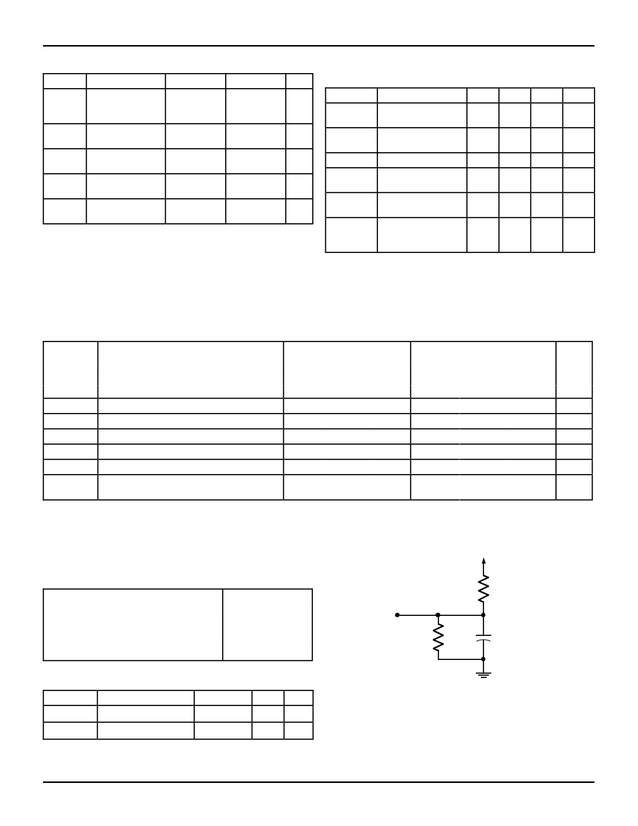
See Figure 8
CAPACITANCE (TA = +25°C, f = 1.0MHz)
2668 tbl 19
Symbol
Parameter
Conditions
CIN (2)
Input Capacitance
VIN = 0V
COUT (1,2) Output Capacitance
VOUT = 0V
NOTES:
1. With output deselected.
2. Characterized values, not currently tested.
Max. Unit
8 pF
12 pF
2668 tbl 20
D.U.T.
680 Ω
1.1 kΩ
30 pF*
or equivalent circuit
2668 drw 09
Figure 8. Output Load
*Includes jig and scope capacitances
5.32
14
Share Link: 