FM1608B Ver la hoja de datos (PDF) - Cypress Semiconductor
Número de pieza
componentes Descripción
Lista de partido
FM1608B Datasheet PDF : 18 Pages
| |||
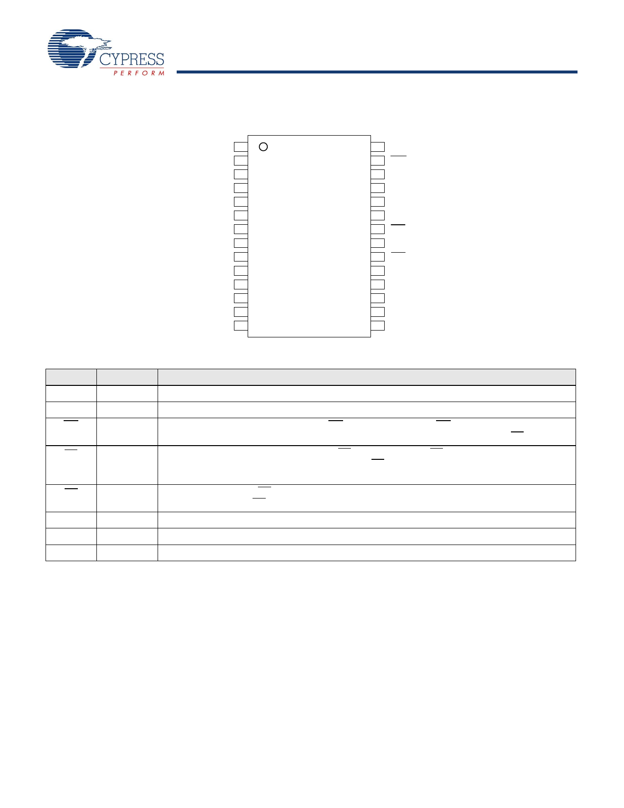
FM1608B
Pinout
NC
A12
A7
A6
A5
A4
A3
A2
A1
A0
DQ0
DQ1
DQ2
VSS
Figure 1. 28-pin SOIC pinout
1
28
2
27
3
26
4
25
5
24
6
28-pin SOIC 23
7
(x 8)
22
8
Top view
21
9 (not to scale) 20
10
19
11
18
12
17
13
16
14
15
VDD
WE
NC
A8
A9
A11
OE
A10
CE
DQ7
DQ6
DQ5
DQ4
DQ3
Pin Definitions
Pin Name I/O Type
Description
A12–A0
DQ7–DQ0
WE
Input Address inputs: The 13 address lines select one of 8,192 bytes in the F-RAM array.
Input/Output Data I/O Lines: 8-bit bidirectional data bus for accessing the F-RAM array.
Input
Write Enable: A write cycle begins when WE is asserted. Asserting WE LOW causes the FM1608B to
write the contents of the data bus to the address location latched by the falling edge of CE.
CE
Input Chip Enable: The device is selected when CE is LOW. Asserting CE LOW causes the address to be
latched internally. Address changes that occur after CE goes LOW will be ignored until the next falling
edge occurs.
OE
Input Output Enable: When OE is LOW, the FM1608B drives the data bus when the valid read data is
available. Deasserting OE HIGH tristates the DQ pins.
VSS
Ground Ground for the device. Must be connected to the ground of the system.
VDD Power supply Power supply input to the device.
NC
No connect No connect. This pin is not connected to the die.
Document Number: 001-86211 Rev. *C
Page 3 of 18
Share Link: 