STM1061 Ver la hoja de datos (PDF) - STMicroelectronics
Número de pieza
componentes Descripción
Lista de partido
STM1061 Datasheet PDF : 21 Pages
| |||
STM1061
PIN DESCRIPTIONS
See Figure 2., page 4 and Table 1., page 4 for a
brief overview of the signals connected to this de-
vice.
OUT (Open Drain). This is the Open Drain Out-
put. It goes low when VCC drops below VTH–, and
remains low as long as VCC is below VTH– +
VHYST.
VCC. This is the Supply voltage and input for the
Voltage Detector.
VSS. Ground, VSS, is the reference for the power
supply. It must be connected to the system
ground.
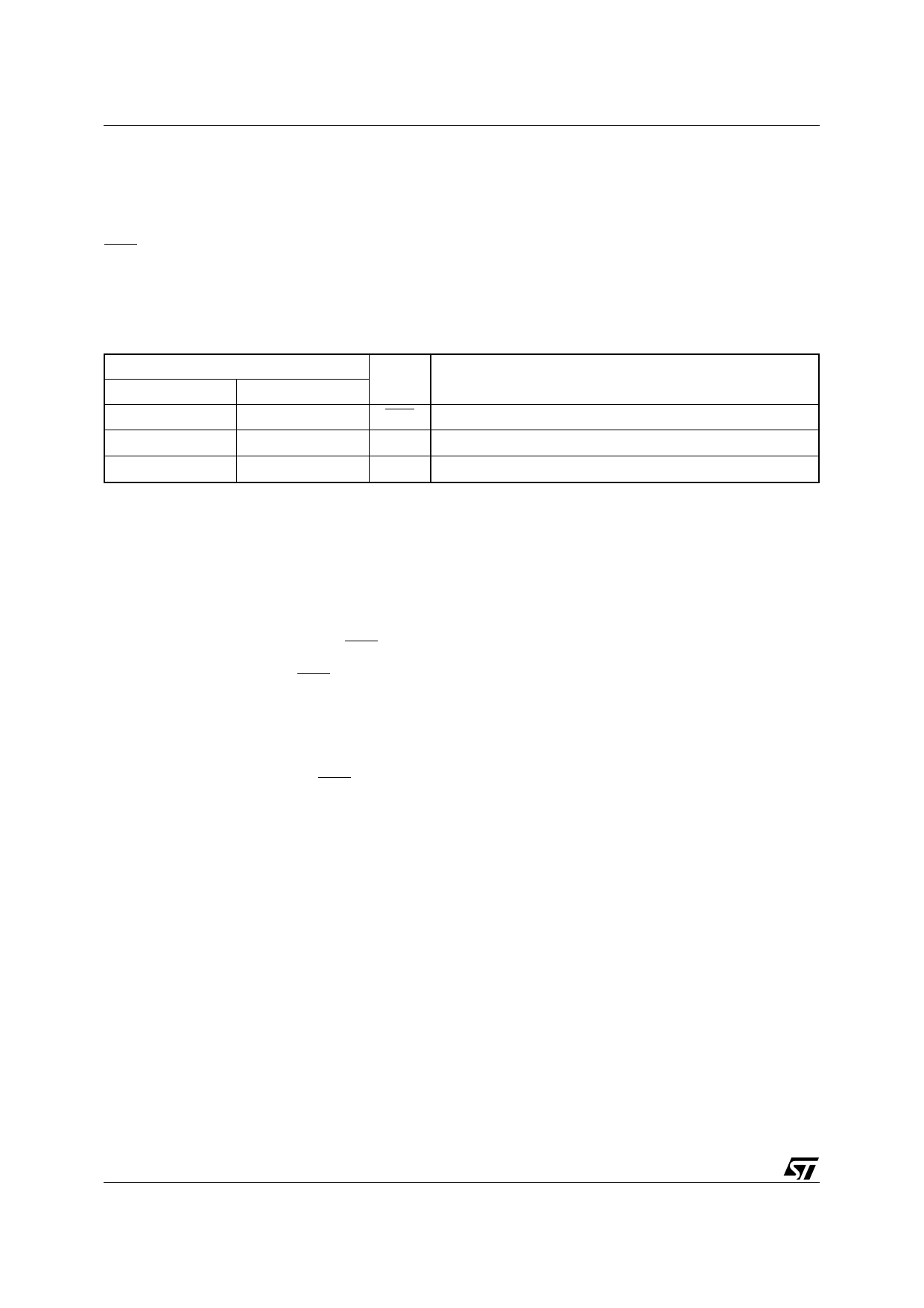
Table 2. Pin Functions
Pin
SOT23-3
SOT323-3 (SC70-3)
1
2
3
3
2
1
Name
OUT
VCC
VSS
Function
Active-Low Open Drain Output
Supply Voltage
Ground
OPERATION
Output
The STM1061 Voltage Detector monitors system
voltages from 1.6V to 5V in 100mV increments.
The detector is designed to ignore fast transients
on VCC and has a voltage hysteresis (VHYST). The
STM1061 asserts an output signal (OUT) whenev-
er VCC goes below the Voltage Detect Threshold
(VTH–). The output signal (OUT) stays asserted
until VCC goes above the Voltage Detect Release
(VTH+). Output voltage (VOUT) is guaranteed valid
down to VCC =0.7V at 25°C.
The STM1061has an open drain active-low output
which will sink current when output is asserted.
Connect a pull-up resistor from OUT to any supply
voltage up to 6V (see Figure 6., page 5). Select a
resistor value large enough to register a logic low,
and small enough to register a logic high while all
of the input current and leakage paths connected
to the reset output line are being supplied. A 10k
pull-up is sufficient in most applications.
The advantages of open drain output is the ability
to connect more open drain outputs in parallel
(wired OR connections) as well as connect the
output to a power supply voltage different from
VCC.
Negative-Going VCC Transients and
Undershoot
The STM1061 device is relatively immune to neg-
ative-going VCC transients (glitches). The graph
(see Figure 11., page 9) indicates the maximum
pulse width a negative VCC transient can have
without causing a reset pulse. As the magnitude of
the transient increases (further below the thresh-
old), the maximum allowable pulse width decreas-
es. Any combination of duration and overdrive
which lies under the curve will NOT generate a re-
set signal.
A 0.1µF bypass capacitor mounted as close as
possible to the VCC pin provides additional tran-
sient immunity.
6/21
Share Link: 