NCV8660C Ver la hoja de datos (PDF) - ON Semiconductor
Número de pieza
componentes Descripción
Lista de partido
NCV8660C Datasheet PDF : 11 Pages
| |||
NCV8660C
DETAILED OPERATING DESCRIPTION
General
The NCV8660C is a 5 V linear regulator providing low
drop−out voltage for 150 mA at low quiescent current levels.
Also featured in this part is a reset output with selectable
delay times. Delay times are selectable via part selection and
control through the Delay Time Select (DT) pin. No pull−up
resistor is needed on the reset output (RO). Pull−up and
pull−down capability are included. Only a small bypass
capacitor on the input (IN) supply pin and output (OUT)
voltage pin are required for normal operation. Thermal
shutdown functionality protects the IC from damage caused
from excessively high temperatures appearing on the IC.
Output Voltage
Output stability is determined by the capacitor selected
from OUT to GND. The NCV8660C has been designed to
work with low ESR (equivalent series resistance) ceramic
capacitors. The device is extremely stable using virtually
any capacitor 2.2 mF and above. Reference the Output
Capacitor Stability graph in Figure 16.
The output capacitor value will affect overshoot during
power−up. A lower value capacitor will cause higher
overshoot on the output. System evaluation should be
performed with minimum loading for evaluation of
overshoot.
Selection of process technology for the NCV8660C
allows for low quiescent current independent of loading.
Quiescent current will remain flat across the entire range of
loads providing a low quiescent current condition in standby
and under heavy loads. This is highly beneficial to systems
requiring microprocessor interrupts during standby mode as
duty cycle and load changes have no impact on the standby
current. Reference Figure 11 for Quiescent Current vs
Output Current.
Current Limit
Current limit is provided on OUT to protect the IC. The
minimum specification is 205 mA. Current limit is specified
under two conditions (OUT = 96% x OUT nominal) and
(OUT = 0 V). No fold−back circuitry exists. Any measured
differences can be attributed to change in die temperature.
The part may be operated up to 205 mA provided thermal die
temperature is considered and is kept below 150°C.
Degradation of electrical parameters at this current is
expected at these elevated levels. A reset (RO) will not occur
with a load less than 205 mA.
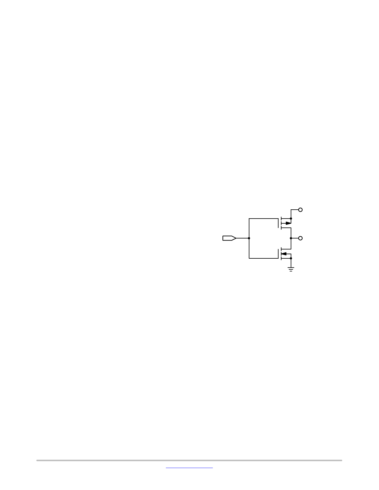
Reset Output
A reset signal is provided on the Reset Output (RO) pin to
provide feedback to the microprocessor of an out of
regulation condition. This is in the form of a logic signal on
RO. Output (OUT) voltage conditions below the RESET
threshold cause RO to go low. The RO integrity is
maintained down to OUT = 1.0 V.
The Reset Output (RO) circuitry includes an active
internal pullup to the output (OUT) as shown in Figure 18.
No external pullup is neccessary.
OUT
RO
Reset
Control
Signal
Figure 18. Reset Output Circuitry
www.onsemi.com
8
Share Link: 