A29010B Ver la hoja de datos (PDF) - AMIC Technology
Número de pieza
componentes Descripción
Lista de partido
A29010B Datasheet PDF : 30 Pages
| |||
A29010B Series
Absolute Maximum Ratings*
Ambient Operating Temperature ..……………. -55°C to +125°C
Storage Temperature …………………………... -65°C to +125°C
Ground to VCC …………………………………….. -2.0V to 6.5V
Output Voltage (Note 1) …………………………… -2.0V to 6.5V
A9 & OE (Note 2) …………………………………. -2.0V to 11.5V
All other pins (Note 1)……………………………….. -2.0V to 6.5V
Output Short Circuit Current (Note 3) ……………………. 200mA
Notes:
1. Minimum DC voltage on input or I/O pins is -0.5V. During
voltage transitions, inputs may undershoot VSS to -2.0V for
periods of up to 20ns. Maximum DC voltage on output and
I/O pins is VCC +0.5V. During voltage transitions, outputs
may overshoot to VCC +1.5V for periods up to 20ns.
2. Minimum DC input voltage on A9 pins is -0.5V. During
voltage transitions, A9 and OE may overshoot VSS to -2.0V
for periods of up to 20ns. Maximum DC input voltage on A9
and OE is +11.5V which may overshoot to 12.5V for
periods up to 20ns.
3. No more than one output is shorted at a time. Duration of
the short circuit should not be greater than one second.
*Comments
Stresses above those listed under "Absolute Maximum Ratings"
may cause permanent damage to this device. These are stress
ratings only. Functional operation of this device at these or any
other conditions above those indicated in the operational
sections of these specification is not implied or intended.
Exposure to the absolute maximum rating conditions for
extended periods may affect device reliability.
Operating Ranges
Commercial Devices
Ambient Temperature (TA) ………………………… 0°C to +70°C
Extended Range Devices
Ambient Temperature (TA) ……………………… -40°C to +85°C
VCC Supply Voltages
VCC for ± 10% devices …………………………. +4.5V to +5.5V
Operating ranges define those limits between which the
functionally of the device is guaranteed.
Device Bus Operations
This section describes the requirements and use of the device
bus operations, which are initiated through the internal
command register. The command register itself does not
occupy any addressable memory location. The register is
composed of latches that store the commands, along with the
address and data information needed to execute the command.
The contents of the register serve as inputs to the internal state
machine. The state machine outputs dictate the function of the
device. The appropriate device bus operations table lists the
inputs and control levels required, and the resulting output. The
following subsections describe each of these operations in
further detail.
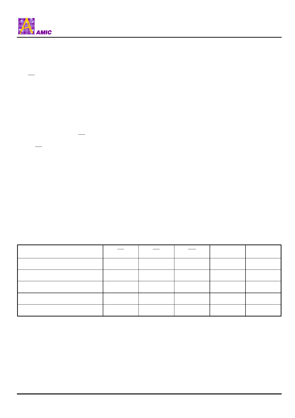
Table 1. A29010B Device Bus Operations
Operation
CE
OE
WE
A0 – A16
I/O0 - I/O7
Read
L
L
H
AIN
DOUT
Write
L
H
L
AIN
DIN
CMOS Standby
VCC ± 0.5 V
X
X
X
High-Z
TTL Standby
H
X
X
X
High-Z
Output Disable
L
H
H
X
High-Z
Legend:
L = Logic Low = VIL, H = Logic High = VIH, VID = 10.5 ± 1.0V, X = Don't Care, DIN = Data In, DOUT = Data Out, AIN = Address In
PRELIMINARY (June, 2016, Version 0.0)
4
AMIC Technology, Corp.
Share Link: 