RF2629 Ver la hoja de datos (PDF) - RF Micro Devices
Número de pieza
componentes Descripción
Lista de partido
RF2629 Datasheet PDF : 6 Pages
| |||
RF2629
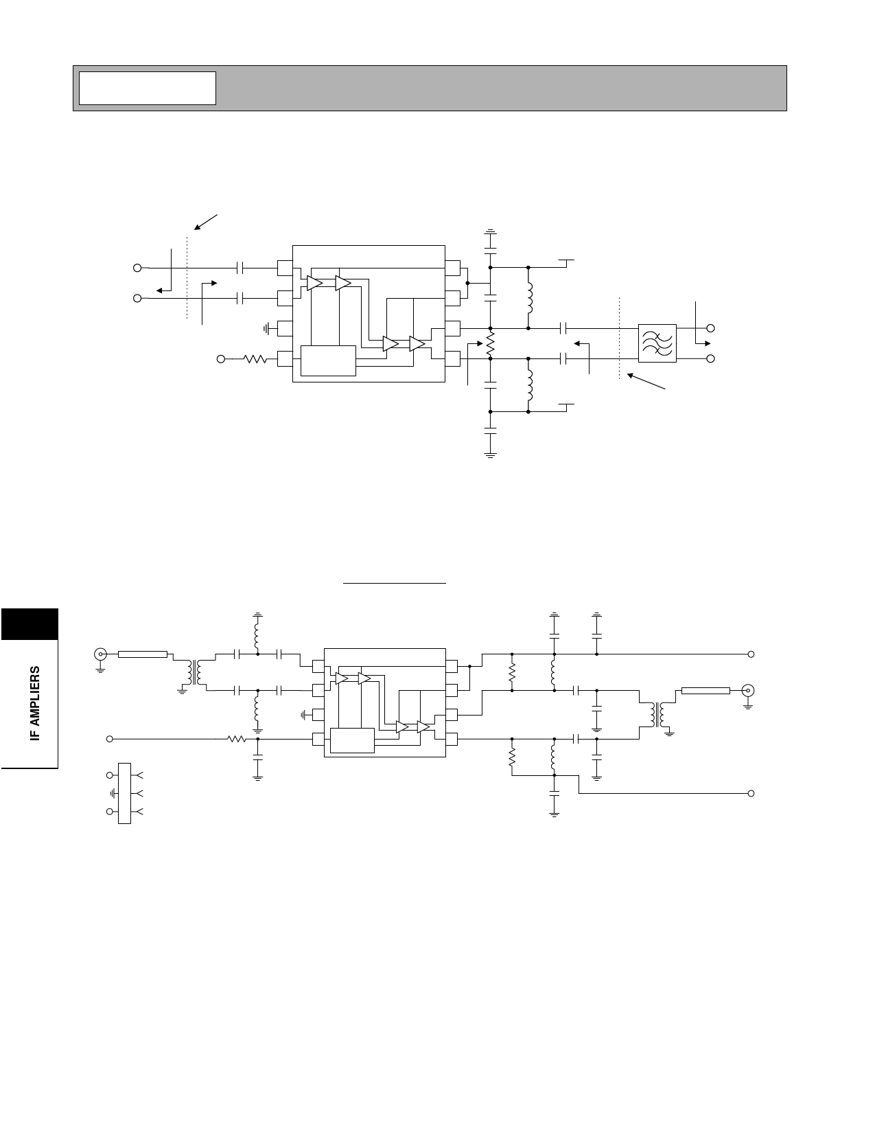
Application Schematic
Measurement
Reference Plane
ZS=1 kΩ
IN+
IN-
10 nF
1
10 nF
2
ZIN=1 kΩ
3
GAIN
4
GAIN
3.3 kΩ
CONTROL
8
7
6
5
ZLOAD,EFF=500 Ω
R2 sets the balanced output impedance to 1 k Ω . L1 and C2
serve dual purposes. L1 serves as an output bias choke, and C2
serves as a series DC block. In addition, the values of L1 and
C2 may be chosen to form an impedance matching network if
the load impedance is not 1 k Ω . Otherwise, the values of L1 and
C1 are chosen to form a parallel-resonant tank circuit at the IF
when the IF filter's input impedance is 1 k Ω.
10 nF
VCC
C1 L1
C2
R2:
1 kΩ
C2
C1
L1 ZOUT=1 kΩ
VCC
10 nF
ZLOAD=1 kΩ
CDMA Filter
OUT+
OUT-
Measurement
Reference Plane
Evaluation Board Schematic
(Download Bill of Materials from www.rfmd.com.)
10
CDMA
J1
50 Ω µ strip
SMA
T1
1
GC
P1
P1-1 1 VCC
2 GND
P1-3 3
GC
C3
5 pF
L1
270 nH
C4
5 pF
C1
10 nF
L2
270 nH
C2
10 nF
R1
3.3 kΩ
C5
1 nF
1
2
3
4
GAIN
CONTROL
2629400, Rev A
C7
10 nF
C10
10 nF
VCC
8
R3
L4
C8
510 Ω 100nH 33 pF
OUT
7
J2
C11
T2
50 Ω µ strip
SMA
6
C9
33 pF
22 pF
1
5
R2
510 Ω
L3
100nH
C12
22 pF
C6
10 nF
VCC
10-42
Rev B4 010720
Share Link: 