EL4584 Ver la hoja de datos (PDF) - Renesas Electronics
Número de pieza
componentes Descripción
Lista de partido
EL4584 Datasheet PDF : 15 Pages
| |||
EL4584
TABLE 4. XTAL VCO COMPONENT VALUES
(APPROXIMATE) (Continued)
FREQUENCY
R1
C1
(MHz)
(k)
(pF)
17.734
300
15
10.738
300
15
12.273
300
15
14.318
300
15
C2
(µF)
0.001
0.001
0.001
0.001
The above oscillators are arranged as Colpitts oscillators,
and the structure is redrawn here to emphasize the split
capacitance used in a Colpitts oscillator. It should be noted
that this oscillator configuration is just one of literally
hundreds possible, and the configuration shown here does
not necessarily represent the best solution for all
applications. Crystal manufacturers are very informative
sources on the design and use of oscillators in a wide variety
of applications, and the reader is encouraged to become
familiar with them.
FIGURE 14. COLPITTS OSCILLATOR
C1 is to adjust the center frequency, C2 DC isolates the
control from the oscillator, and V1 is the primary control
device. C2 should be much larger than CV so that V1 has
maximum modulation capability. The frequency of oscillation
is given by Equations 5 and 6:
F = ------------1--------------
12 LCT
(EQ. 5)
CT = ---C-----1---C----2-------+----C----C-1---C1----C2----CV----V----+-------C----2----C----V-----
(EQ. 6)
Choosing Loop Filter Components
The PLL, VCO, and loop filter can be represented in Figure 15:
FIGURE 15.
FN7174 Rev 3.00
May 9, 2008
Where:
Kd = phase detector gain in A/rad
F(s) = loop filter impedance in V/A
KVCO = VCO gain in rad/s/V
N = internal or external divisor
It can be shown that for the loop filter shown in Equation 7:
C3 = -K----d-N--K----V----2nC----O--- C4 = C-1---0-3- R3 = K---2--d--N-K----V----C---n-O---
(EQ. 7)
Where n = loop filter bandwidth, and = loop filter damping
factor.
1. Kd = 300µA/2rad = 4.77e-5A/rad for the EL4584.
2. The loop bandwidth should be about HSYNC
frequency/20, and the damping ratio should be 1 for
optimum performance. For our example,
n = 15.734kHz/20 = 787Hz5000rad/S.
3. N = 910 from Table 2.
N = H------–--V---S-C---Y--O---N--f--r-C--e--f--qr---eu----qe----un---e-c---ny----c---y-- = 1-1---4-5--.-.-3-7--1-3---84---1-2--8-6---M-k-- = 910
(EQ. 8)
4. KVCO represents how much the VCO frequency changes
for each volt applied at the control pin. It is assumed (but
probably is not) linear about the lock point (2.5V). Its
value depends on the VCO configuration and the varactor
transfer function CV = F(VC), where VC is the reverse
bias control voltage, and CV is varactor capacitance.
Since F(VC) is nonlinear, it is probably best to build the
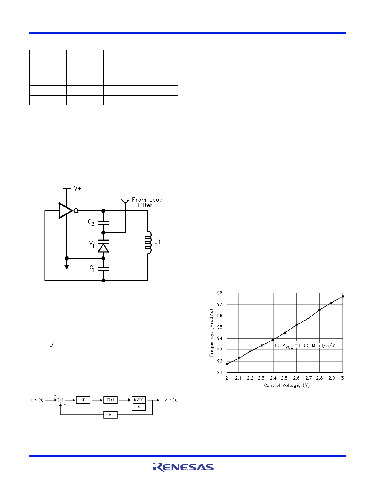
VCO and measure KVCO about 2.5V. The results of one
such measurement are shown in the following. The slope
of the curve is determined by linear regression
techniques and equals KVCO. For our example,
KVCO = 6.05 Mrad/S/V.
FIGURE 16. FOSC vs VC, LC VCO
5. Now we can solve for C3, C4, and R3. We choose
R3 = 30k for convenience.
6. Notice R2 has little effect on the loop filter design. R2
should be large, around 100k, and can be adjusted to
compensate for any static phase error t at lock, but if
made too large, will slow loop response. If R2 is made
Page 10 of 15
Share Link: 