DT28F320J5-120 Ver la hoja de datos (PDF) - Intel
Número de pieza
componentes Descripción
Lista de partido
DT28F320J5-120 Datasheet PDF : 51 Pages
| |||
28F320J5 and 28F640J5
Three CE pins are used to enable and disable the device. A unique CE logic design (see Table 2,
“Chip Enable Truth Table” on page 12) reduces decoder logic typically required for multi-chip
designs. External logic is not required when designing a single chip, a dual chip, or a 4-chip
miniature card or SIMM module.
The BYTE# pin allows either x8 or x16 read/writes to the device. BYTE# at logic low selects 8-bit
mode; address A0 selects between the low byte and high byte. BYTE# at logic high enables 16-bit
operation; address A1 becomes the lowest order address and address A0 is not used (don’t care). A
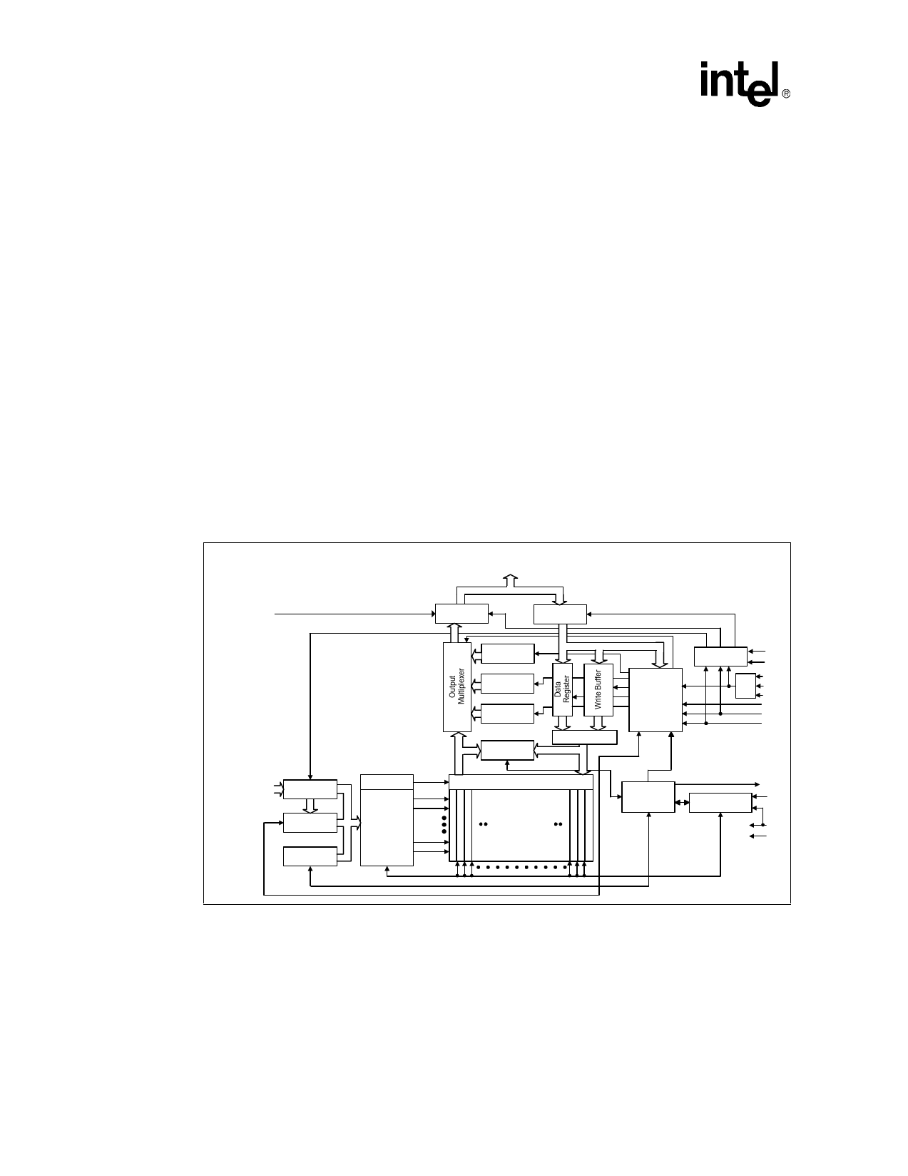
device block diagram is shown in Figure 1.
When the device is disabled (see Table 2 on page 12) and the RP# pin is at VCC, the standby mode
is enabled. When the RP# pin is at GND, a further power-down mode is enabled which minimizes
power consumption and provides write protection during reset. A reset time (tPHQV) is required
from RP# switching high until outputs are valid. Likewise, the device has a wake time (tPHWL)
from RP#-high until writes to the CUI are recognized. With RP# at GND, the WSM is reset and the
status register is cleared.
The Intel StrataFlash memory devices are available in several package types. The 64-Mbit is
available in 56-lead SSOP (Shrink Small Outline Package) and µBGA* package (micro Ball Grid
Array). The 32-Mbit is available in 56-lead TSOP (Thin Small Outline Package) and 56-lead
SSOP. Figures 2, 3, and 4 show the pinouts.
Figure 1. Intel StrataFlash® Memory Block Diagram
DQ0 - DQ15
VCCQ
32-Mbit: A0- A21
64-Mbit: A0 - A22
Input Buffer
Address
Latch
Address
Counter
Y-Decoder
X-Decoder
Output Buffer
Input Buffer
Query
Identifier
Register
Status
Register
Data
Comparator
Y-Gating
Multiplexer
32-Mbit: Thirty-two
64-Mbit: Sixty-four
128-Kbyte Blocks
Command
User
Interface
I/O Logic
CE
Logic
VCC
BYTE#
CE0
CE1
CE2
WE#
OE#
RP#
Write State
Machine
Program/Erase
Voltage Switch
STS
VPEN
VCC
GND
8
Datasheet
Share Link: 