DT28F320J5-120 Ver la hoja de datos (PDF) - Intel
Número de pieza
componentes Descripción
Lista de partido
DT28F320J5-120 Datasheet PDF : 51 Pages
| |||
28F320J5 and 28F640J5
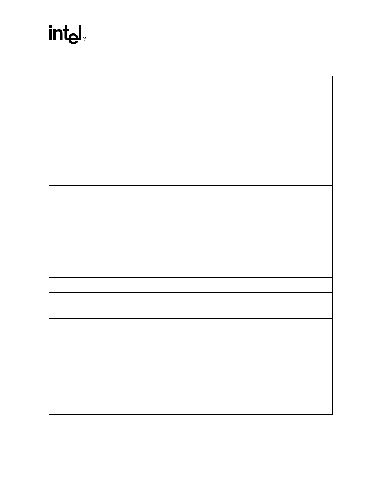
Table 1. Lead Descriptions
Symbol
A0
A1–A22
DQ0–DQ7
DQ8–DQ15
CE0,
CE1,
CE2
RP#
OE#
WE#
STS
BYTE#
VPEN
VCC
VCCQ
GND
NC
Type
INPUT
INPUT
INPUT/
OUTPUT
INPUT/
OUTPUT
INPUT
INPUT
INPUT
INPUT
OPEN
DRAIN
OUTPUT
INPUT
INPUT
SUPPLY
OUTPUT
BUFFER
SUPPLY
SUPPLY
Name and Function
BYTE-SELECT ADDRESS: Selects between high and low byte when the device is in x8 mode.
This address is latched during a x8 program cycle. Not used in x16 mode (i.e., the A0 input buffer
is turned off when BYTE# is high).
ADDRESS INPUTS: Inputs for addresses during read and program operations. Addresses are
internally latched during a program cycle.
32-Mbit: A0–A21
64-Mbit: A0–A22
LOW-BYTE DATA BUS: Inputs data during buffer writes and programming, and inputs
commands during Command User Interface (CUI) writes. Outputs array, query, identifier, or status
data in the appropriate read mode. Floated when the chip is de-selected or the outputs are
disabled. Outputs DQ6–DQ0 are also floated when the Write State Machine (WSM) is busy. Check
SR.7 (status register bit 7) to determine WSM status.
HIGH-BYTE DATA BUS: Inputs data during x16 buffer writes and programming operations.
Outputs array, query, or identifier data in the appropriate read mode; not used for status register
reads. Floated when the chip is de-selected, the outputs are disabled, or the WSM is busy.
CHIP ENABLES: Activates the device’s control logic, input buffers, decoders, and sense
amplifiers. When the device is de-selected (see Table 2 on page 12, power reduces to standby
levels.
All timing specifications are the same for these three signals. Device selection occurs with the first
edge of CE0, CE1, or CE2 that enables the device. Device deselection occurs with the first edge of
CE0, CE1, or CE2 that disables the device (see Table 2).
RESET/ POWER-DOWN: Resets internal automation and puts the device in power-down mode.
RP#-high enables normal operation. Exit from reset sets the device to read array mode. When
driven low, RP# inhibits write operations which provides data protection during power transitions.
RP# at VHH enables master lock-bit setting and block lock-bits configuration when the master
lock-bit is set. RP# = VHH overrides block lock-bits thereby enabling block erase and
programming operations to locked memory blocks. Do not permanently connect RP# to VHH.
OUTPUT ENABLE: Activates the device’s outputs through the data buffers during a read cycle.
OE# is active low.
WRITE ENABLE: Controls writes to the Command User Interface, the Write Buffer, and array
blocks. WE# is active low. Addresses and data are latched on the rising edge of the WE# pulse.
STATUS: Indicates the status of the internal state machine. When configured in level mode
(default mode), it acts as a RY/BY# pin. When configured in one of its pulse modes, it can pulse to
indicate program and/or erase completion. For alternate configurations of the STATUS pin, see
the Configurations command. Tie STS to VCCQ with a pull-up resistor.
BYTE ENABLE: BYTE# low places the device in x8 mode. All data is then input or output on
DQ0–DQ7, while DQ8–DQ15 float. Address A0 selects between the high and low byte. BYTE# high
places the device in x16 mode, and turns off the A0 input buffer. Address A1 then becomes the
lowest order address.
ERASE / PROGRAM / BLOCK LOCK ENABLE: For erasing array blocks, programming data, or
configuring lock-bits.
With VPEN ≤ VPENLK, memory contents cannot be altered.
DEVICE POWER SUPPLY: With VCC ≤ VLKO, all write attempts to the flash memory are inhibited.
OUTPUT BUFFER POWER SUPPLY: This voltage controls the device’s output voltages. To
obtain output voltages compatible with system data bus voltages, connect VCCQ to the system
supply voltage.
GROUND: Do not float any ground pins.
NO CONNECT: Lead is not internally connected; it may be driven or floated.
Datasheet
9
Share Link: 