IRF440 Ver la hoja de datos (PDF) - Intersil
Número de pieza
componentes Descripción
Lista de partido
IRF440 Datasheet PDF : 7 Pages
| |||
IRF440
Absolute Maximum Ratings TC = 25oC, Unless Otherwise Specified
Drain To Source Voltage (Note 1) . . . . . . . . . . . . . . . . . . . . . . . . . . . . . . . . . . . . . . . . . . . . . VDS
Drain To Gate Voltage (RGS = 20kΩ) (Note 1). . . . . . . . . . . . . . . . . . . . . . . . . . . . . . . . . . . VDGR
Continuous Drain Current . . . . . . . . . . . . . . . . . . . . . . . . . . . . . . . . . . . . . . . . . . . . . . . . . . . . . ID
TC = 100oC . . . . . . . . . . . . . . . . . . . . . . . . . . . . . . . . . . . . . . . . . . . . . . . . . . . . . . . . . . . . . . ID
Pulsed Drain Current (Note 3) . . . . . . . . . . . . . . . . . . . . . . . . . . . . . . . . . . . . . . . . . . . . . . . . . IDM
Gate To Source Voltage . . . . . . . . . . . . . . . . . . . . . . . . . . . . . . . . . . . . . . . . . . . . . . . . . . . . . VGS
Maximum Power Dissipation . . . . . . . . . . . . . . . . . . . . . . . . . . . . . . . . . . . . . . . . . . . . . . . . . . PD
Linear Derating Factor . . . . . . . . . . . . . . . . . . . . . . . . . . . . . . . . . . . . . . . . . . . . . . . . . . . . . . . .
Single Pulse Avalanche Energy Rating (Note 4) . . . . . . . . . . . . . . . . . . . . . . . . . . . . . . . . . . EAS
Operating and Storage Temperature . . . . . . . . . . . . . . . . . . . . . . . . . . . . . . . . . . . . . . . .TJ, TSTG
Maximum Temperature for Soldering
Leads at 0.063in (1.6mm) from Case for 10s. . . . . . . . . . . . . . . . . . . . . . . . . . . . . . . . . . . . . TL
Package Body for 10s, See Techbrief 334 . . . . . . . . . . . . . . . . . . . . . . . . . . . . . . . . . . . . . Tpkg
IRF440
500
500
8.0
5.0
32
±20
125
1.0
510
-55 to 150
300
260
UNITS
V
V
A
A
A
V
W
W/oC
A
oC
oC
oC
CAUTION: Stresses above those listed in “Absolute Maximum Ratings” may cause permanent damage to the device. This is a stress only rating and operation of the
device at these or any other conditions above those indicated in the operational sections of this specification is not implied.
NOTE:
1. TJ = 25oC to 125oC.
Electrical Specifications TC = 25oC, Unless Otherwise Specified
PARAMETER
SYMBOL
TEST CONDITIONS
MIN TYP MAX UNITS
Drain To Source Breakdown Voltage
Gate Threshold Voltage
Zero Gate Voltage Drain Current
On-State Drain Current (Note 2)
Gate to Source Leakage Current
Drain to Source On Resistance (Note 2)
Forward Transconductance (Note 2)
Turn-On Delay Time
Rise Time
Turn-Off Delay Time
Fall Time
Total Gate Charge
(Gate to Source + Gate to Drain)
Gate to Source Charge
BVDSS ID = 250µA, VGS = 0V (Figure 10)
500
-
-
V
VGS(TH) VDS = VGS, ID = 250µA
2.0
-
4.0
V
IDSS VDS = Rated BVDSS, VGS = 0V
-
VDS = 0.8 x Rated BVDSS, VGS = 0V, TJ = 125oC
-
-
25
µA
-
250 µA
ID(ON) VDS > ID(ON) x rDS(ON)MAX, VGS = 10V
8.0
-
-
A
IGSS VGS = ±20V
-
- ±100 nA
rDS(ON) ID = 4.4A, VGS = 10V (Figures 8, 9)
- 0.70 0.850 Ω
gfs
VDS = 50V, ID = 4.4A (Figure 12)
4.9 7.5
-
S
td(ON) VDD = 250V, ID ≈ 8.0A, RG = 9.1Ω, RL = 30Ω,
-
15 21
ns
tr
(Figure 17, 18) MOSFET Switching Times are
-
Essentially Independent of Operating Temperature
22 35
ns
td(OFF)
-
49 74
ns
tf
-
20 30
ns
Qg(TOT) VGS = 10V, ID = 8.0A, VDS = 0.8 x Rated BVDSS,
-
Ig(REF) = 1.5mA (Figures 14, 19, 20) Gate Charge is
Qgs Essentially Independent of Operating Temperature
-
42
63
nC
9
-
nC
Gate to Drain “Miller” Charge
Input Capacitance
Output Capacitance
Reverse Transfer Capacitance
Internal Drain Inductance
Qgd
-
22
-
nC
CISS VDS = 25V, VGS = 0V, f = 1MHz (Figure 11)
- 1225 -
pF
COSS
-
200
-
pF
CRSS
-
85
-
pF
LD
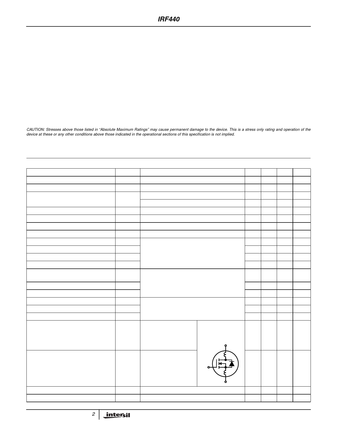
Measured between the
Modified MOSFET
-
5.0
-
nH
Contact Screw on Header Symbol Showing the
that is Closer to Source and Internal Device
Gate Pins and Center of Inductances
Die
D
Internal Source Inductance
LS
Measured from the Source
Lead, 6mm (0.25in) from
LD
- 12.5 -
nH
Header and Source
Bonding Pad
G
LS
Thermal Resistance Junction to Case
Thermal Resistance Junction to Ambient
RθJC
RθJA
Free Air Operation
S
-
-
1.0 oC/W
-
-
30 oC/W
2
Share Link: 