ISL6521 Ver la hoja de datos (PDF) - Renesas Electronics
Número de pieza
componentes Descripción
Lista de partido
ISL6521 Datasheet PDF : 14 Pages
| |||
ISL6521
where: ITRAN is the transient load current step, tRISE is the
response time to the application of load, and tFALL is the
response time to the removal of load. Be sure to check both of
these equations at the minimum and maximum output levels
for the worst case response time.
Input Capacitor Selection
The important parameters for the bulk input capacitors are the
voltage rating and the RMS current rating. For reliable
operation, select bulk input capacitors with voltage and current
ratings above the maximum input voltage and largest RMS
current required by the circuit. The capacitor voltage rating
should be at least 1.25 times greater than the maximum input
voltage and a voltage rating of 1.5 times is a conservative
guideline. The RMS current rating requirement for the input
capacitor of a buck regulator is approximately 1/2 of the
summation of the DC load current.
Use a mix of input bypass capacitors to control the voltage
overshoot across the MOSFETs. Use ceramic capacitance for
the high frequency decoupling and bulk capacitors to supply
the RMS current. Small ceramic capacitors can be placed very
close to the upper MOSFET to suppress the voltage induced in
the parasitic circuit impedances.
For a through-hole design, several electrolytic capacitors may
be needed. For surface mount designs, solid tantalum
capacitors can be used, but caution must be exercised with
regard to the capacitor surge current rating. These capacitors
must be capable of handling the surge-current at power-up.
Transistors Selection/Considerations
The ISL6521 can employ up to 5 external transistors. Two
N-channel MOSFETs are used in the synchronous-rectified
buck topology of PWM converter. The linear controllers can
each drive an NPN bipolar transistor as a pass element. All
these transistors should be selected based upon rDS(ON) ,
current gain, saturation voltages, gate/base supply
requirements, and thermal management considerations.
PWM MOSFET Selection and Considerations
In high-current PWM applications, the MOSFET power
dissipation, package selection and heatsink are the dominant
design factors. The power dissipation includes two loss
components; conduction loss and switching loss. These losses
are distributed between the upper and lower MOSFETs
according to duty factor (see the equations below). The
conduction losses are the main component of power
dissipation for the lower MOSFETs. Only the upper MOSFET
has significant switching losses, since the lower device turns
on and off into near zero voltage.
The equations below assume linear voltage-current transitions
and do not model power loss due to the reverse-recovery of
the lower MOSFET’s body diode. The gate-charge losses are
dissipated by the ISL6521 and don't heat the MOSFETs.
However, large gate-charge increases the switching time, tSW
which increases the upper MOSFET switching losses. Ensure
that both MOSFETs are within their maximum junction
temperature at high ambient temperature by calculating the
temperature rise according to package thermal-resistance
specifications. A separate heatsink may be necessary
depending upon MOSFET power, package type, ambient
temperature and air flow.
PUPPER = I--O-----2---------r--D----S----V--O--I--N-N------------V----O-----U----T-- + I--O-----------V----I--N------2----t--S----W-----------F----S--
PLOWER = I--O-----2---------r--D----S------O-----N---V-----I-N------V----I--N-----–----V-----O----U----T----
Given the reduced available gate bias voltage (5V) logic-level
or sub-logic-level transistors have to be used for both N-
MOSFETs. Caution should be exercised with devices
exhibiting very low VGS(ON) characteristics, as the low gate
threshold could be conducive to some shoot-through (due to
the Miller effect), in spite of the counteracting circuitry present
aboard the ISL6521.
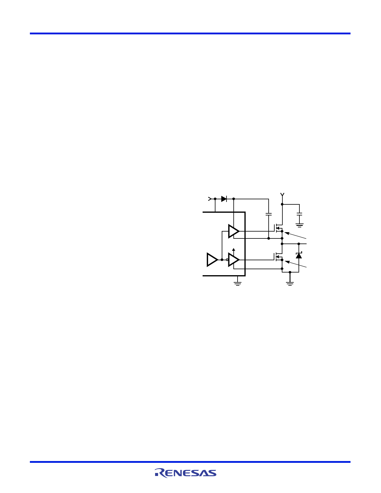
+5V
VCC
ISL6521
BOOT
CBOOT
UGATE
PHASE
VCC
+-
LGATE
PGND
GND
+5V OR LESS
+
Q1
NOTE:
VGS VCC -0.5V
Q2
CR1
NOTE:
VGS VCC
FIGURE 8. MOSFET GATE BIAS
Rectifier CR1 is a clamp that catches the negative inductor
swing during the dead time between the turn off of the lower
MOSFET and the turn on of the upper MOSFET. The diode
must be a Schottky type to prevent the lossy parasitic
MOSFET body diode from conducting. It is acceptable to omit
the diode and let the body diode of the lower MOSFET clamp
the negative inductor swing, providing the body diode is fast
enough to avoid excessive negative voltage swings at the
PHASE pin. The diode's rated reverse breakdown voltage
must be greater than the maximum input voltage.
Linear Controller Transistor Selection
The main criteria for selection of transistors for the linear
regulators is package selection for efficient removal of heat.
The power dissipated in a linear regulator is:
PLINEAR = IO VIN – VOUT
FN9148 Rev 2.00
Feb 8, 2005
Page 11 of 14
Share Link: 