BR25G128FVM-3GTR Ver la hoja de datos (PDF) - ROHM Semiconductor
Número de pieza
componentes Descripción
Lista de partido
BR25G128FVM-3GTR Datasheet PDF : 36 Pages
| |||
BR25G128-3
Datasheet
I/O Peripheral Circuits
In order to realize stable high speed operations, pay attention to the following input / output pin conditions.
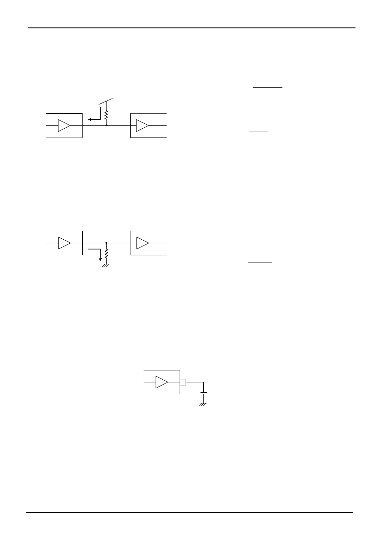
Input pin pull up, pull down resistance
When to attach pull up, pull down resistance to EEPROM input pin, select an appropriate value for the microcontroller VOL,
IOL with considering VIL characteristics of this IC.
1. Pull Up Resistance
Vcc-VOLM
RPU ≥
IOLM
・・・①
Microcontroller IOLM
RPU
VOLM
EEPROM
VILE
“L” output
“L” input
Figure 49. Pull up resistance
VOLM ≤ VILM ・・・②
Example) When Vcc=5V, VILE=1.5V, VOLM=0.4V, IOLM=2mA,
from the equation ①,
RPU
≥
5‐0.4
2 ×10‐3
∴ RPU ≥ 2.3[kΩ]
With the value of Rpu to satisfy the above equation, VOLM
becomes 0.4V or lower, and with VILE (=1.5V), the equation ② is
also satisfied.
・VILE :EEPROM VIL specifications
・VOLM :Microcontroller VOL specifications
・IOLM :Microcontroller IOL specifications
And, in order to prevent malfunction or erroneous write at power ON/OFF, be sure to make CSB pull up.
2. Pull Down Resistance
VOHM
RPD ≥ IOHM
・・・③
Microcontroller
VOHM
“H” output
IOHM
RPD
EEPROM
VIHE
“H” input
Figure 50. Pull down resistance
VOLM ≤ VIHM ・・・④
Example) When VCC=5V, VOHM=VCC-0.5V, IOHM=0.4mA,
VIHE=VCC×0.7V, from the equation③,
RPD
≥
5‐0.5
0.4 ×10‐3
∴RPD ≥ 11.3[kΩ]
Further, by amplitude VIHE, VILE of signal input to EEPROM, operation speed changes. By inputting Vcc/GND level
amplitude of signal, more stable high speed operations can be realized. On the contrary, when amplitude of 0.8VCC /
0.2Vcc is input, operation speed becomes slow. (Note1)
In order to realize more stable high speed operation, it is recommended to make the values of RPU, RPD as large as
possible, and make the amplitude of signal input to EEPROM close to the amplitude of VCC / GND level.
(Note1) In this case, guaranteed value of operating timing is guaranteed.
3. SO Load Capacity Condition
Load capacity of SO output pin affects upon delay characteristic of SO output (Data output delay time, time from HOLDB
to High-Z, Output rise time, Output fall time.). In order to make output delay characteristic into better, make SO load
capacity small.
EEPROM
SO
CL
Figure 51. SO load capacity
4. Other cautions
Make the each wire length from the microcontroller to EEPROM input pin same length, in order to prevent setup / hold
violation to EEPROM, owing to difference of wire length of each input.
www.rohm.com
©2014 ROHM Co., Ltd. All rights reserved.
TSZ22111・15・001
19/32
TSZ02201-0R2R0G100670-1-2
19.Mar.2014 Rev.001
Share Link: 