L9904(2002) Ver la hoja de datos (PDF) - STMicroelectronics
Número de pieza
componentes Descripción
Lista de partido
L9904 Datasheet PDF : 17 Pages
| |||
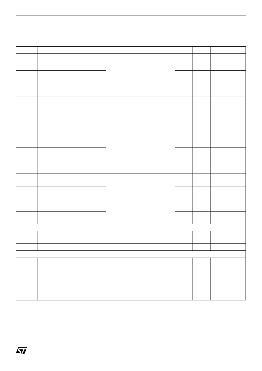
ELECTRICAL CHARACTERISTICS (continued)
Symbol
Parameter
Test Condition
Drivers for external lowside power MOS
RGL1L ON-resistance of SINK stage
RGL2L
IGLX = 50mA; TJ = 25°C
IGLX = 50mA; TJ = 125°C
RGL1H, ON-resistance of SOURCE stage IGLX = -50mA; TJ = 25°C
RGL2H
IGLX = -50mA; TJ = 125°C
VGL1H, Gate ON voltage (SOURCE)
VGL2H
VVS = 8V; IGLX = 0
VVS = 13.5V; IGLX = 0
VVS = 20V; IGLX = 0
RGL1 Gate discharge resistance
RGL2
EN = LOW
2. not tested in production: guaranteed by design and verified in characterization
Timing of the drivers
tGH1LH Propagation delay time
tGH2LH
Fig. 2
VVS = 13.5V
VS1 = VS2 =0
CCBX = 0.1µF
tGH1LH
tGH2LH
tGH1HL
tGH2HL
tGL1LH
tGL2LH
RPR= 10kW
Propagation delay time including
cross conduction protection time
tCCP
Propagation delay time
Fig. 2
VVS = 13.5V
VS1 = VS2 =0
CCBX = 0.1µF
CPR= 150pF;
RPR= 10kΩ;
5)
Propagation delay time
Fig. 2
VVS = 13.5V
VS1 = VS2 =0
CCBX = 0.1µF
tGL1LH
tGL2LH
tGL1HL
tGL2HL
tGH1r
tGH2r
tGH1f
tGH2f
tGL1r
tGL2r
tGL1f
tGL2f
RPR= 10kΩ
Propagation delay time including
cross conduction protection time
tCCP
Propagation delay time
Fig. 2
VVS = 13.5V
VS1 = VS2 =0
CCBX = 0.1µF
CPR= 150pF;
RPR= 10kΩ;
5)
Rise time
Fall time
Fig. 2
VVS = 13.5V
VS1 = VS2 =0
CCBX = 0.1µF
Rise time
Fall time
CGHX = 4.7nF
CGLX = 4.7nF
RPR= 10kΩ;
L9904
Min. Typ. Max. Unit
10
Ω
20
Ω
10
Ω
20
Ω
7V
VVS
10V
VVS
10V
14V
10
100
kΩ
500
ns
0.7
1
1.3
µs
500
ns
500
ns
0.7
1
1.3
µs
500
ns
1
µs
1
µs
1
µs
1
µs
7/17
Share Link: 