IRFZ44ZS Ver la hoja de datos (PDF) - International Rectifier
Número de pieza
componentes Descripción
Lista de partido
IRFZ44ZS Datasheet PDF : 12 Pages
| |||
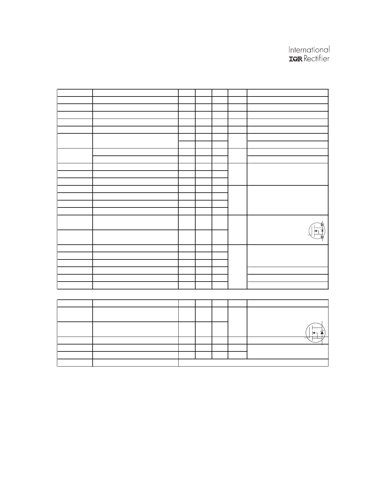
IRFZ44Z/S/L
Static @ TJ = 25°C (unless otherwise specified)
V(BR)DSS
∆ΒVDSS/∆TJ
RDS(on)
VGS(th)
Parameter
Min.
Drain-to-Source Breakdown Voltage 55
Breakdown Voltage Temp. Coefficient –––
Static Drain-to-Source On-Resistance –––
Gate Threshold Voltage
2.0
Typ. Max.
––– –––
0.054 –––
11.1 13.9
––– 4.0
Units
Conditions
V VGS = 0V, ID = 250µA
f V/°C Reference to 25°C, ID = 1mA
mΩ VGS = 10V, ID = 31A
V VDS = VGS, ID = 250µA
gfs
Forward Transconductance
22 ––– ––– S VDS = 25V, ID = 31A
IDSS
Drain-to-Source Leakage Current
––– ––– 20 µA VDS = 55V, VGS = 0V
––– ––– 250
VDS = 55V, VGS = 0V, TJ = 125°C
IGSS
Gate-to-Source Forward Leakage
––– ––– 200 nA VGS = 20V
Gate-to-Source Reverse Leakage
––– ––– -200
VGS = -20V
Qg
Total Gate Charge
––– 29 43 nC ID = 31A
Qgs
Qgd
Gate-to-Source Charge
Gate-to-Drain ("Miller") Charge
––– 7.2 11
––– 12 18
f VDS = 44V
VGS = 10V
td(on)
Turn-On Delay Time
––– 14 ––– ns VDD = 28V
tr
Rise Time
––– 68 –––
ID = 31A
td(off)
tf
Turn-Off Delay Time
Fall Time
––– 33 –––
––– 41 –––
f RG = 15Ω
VGS = 10V
LD
Internal Drain Inductance
––– 4.5 ––– nH Between lead,
D
6mm (0.25in.)
LS
Internal Source Inductance
––– 7.5 –––
from package
G
Ciss
Coss
Crss
Coss
Coss
Coss eff.
Input Capacitance
Output Capacitance
Reverse Transfer Capacitance
Output Capacitance
Output Capacitance
Effective Output Capacitance
––– 1420 –––
––– 240 –––
––– 130 –––
––– 830 –––
––– 190 –––
––– 300 –––
and center of die contact
S
pF VGS = 0V
VDS = 25V
ƒ = 1.0MHz, See Fig. 5
VGS = 0V, VDS = 1.0V, ƒ = 1.0MHz
VGS = 0V, VDS = 44V, ƒ = 1.0MHz
VGS = 0V, VDS = 0V to 44V
Diode Characteristics
Parameter
IS
Continuous Source Current
Min. Typ. Max. Units
Conditions
––– ––– 51
MOSFET symbol
(Body Diode)
ISM
Pulsed Source Current
à (Body Diode)
VSD
Diode Forward Voltage
trr
Reverse Recovery Time
Qrr
Reverse Recovery Charge
––– ––– 200
––– ––– 1.2
––– 23 35
––– 17 26
A showing the
D
integral reverse
f p-n junction diode.
G
V TJ = 25°C, IS = 31A, VGS = 0V
S
f ns TJ = 25°C, IF = 31A, VDD = 28V
nC di/dt = 100A/µs
ton
Forward Turn-On Time
Intrinsic turn-on time is negligible (turn-on is dominated by LS+LD)
Notes:
Repetitive rating; pulse width limited by
max. junction temperature. (See fig. 11).
Limited by TJmax, starting TJ = 25°C, L =0.18mH,
RG = 25Ω, IAS = 31A, VGS =10V. Part not
recommended for use above this value.
ISD ≤ 31A, di/dt ≤ 840A/µs, VDD ≤ V(BR)DSS,
TJ ≤ 175°C.
Pulse width ≤ 1.0ms; duty cycle ≤ 2%.
Coss eff. is a fixed capacitance that gives the same charging time
as Coss while VDS is rising from 0 to 80% VDSS .
Limited by TJmax , see Fig.12a, 12b, 15, 16 for typical repetitive
avalanche performance.
This value determined from sample failure population. 100%
tested to this value in production.
This is applied to D2Pak, when mounted on 1" square PCB
( FR-4 or G-10 Material ). For recommended footprint and
soldering techniques refer to application note #AN-994.
Rθ is rated at TJ of approximately 90°C.
2
www.irf.com
Share Link: 