VNP35N07FI(2013) Ver la hoja de datos (PDF) - STMicroelectronics
Número de pieza
componentes Descripción
Lista de partido
VNP35N07FI Datasheet PDF : 13 Pages
| |||
VNP35N07FI-VNB35N07-VNV35N07
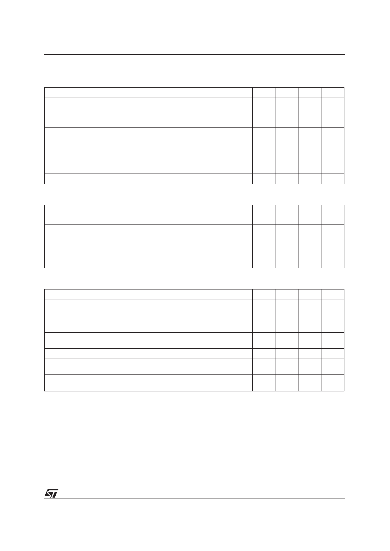
ELECTRICAL CHARACTERISTICS (continued)
SWITCHING (∗∗)
Symb ol
P a ram et er
Test Conditions
Min. Typ . Max. Un it
td(on)
tr
td(off)
tf
Turn-on Delay Time
Rise Time
Turn-off Delay Time
Fall Time
VDD = 28 V
Vgen = 10 V
(see figure 3)
Id = 18 A
Rgen = 10 Ω
100 200
ns
350 600
ns
650 1000 ns
200 350
ns
td(on) Turn-on Delay Time
VDD = 28 V
Id = 18 A
500 800
ns
tr
Rise Time
Vgen = 10 V
Rgen = 1000 Ω
2.7
4.2
µs
td(off) Turn-off Delay Time
(see figure 3)
10
16
µs
tf
Fall Time
4.3
6.5
µs
(di/ dt) on
t(s) Qi
Turn-on Current Slope
Total Input Charge
VDD = 28 V
Vin = 10 V
VDD = 12 V
ID = 18 A
Rgen = 10 Ω
ID = 18 A Vin = 10 V
60
A/µs
100
nC
uc SOURCE DRAIN DIODE
rod Symbol
P VSD (∗)
te trr(∗∗)
ole Qrr(∗∗)
Obs IRRM(∗∗)
P a ram et er
Forward O n Voltage
Reverse Recovery
Time
Reverse Recovery
Charge
Reverse Recovery
Cu r re nt
Test Conditions
ISD = 18 A Vin = 0
ISD = 18 A di/dt = 100 A/µs
VDD = 30 V Tj = 25 oC
(see test circuit, figure 5)
Min.
Typ .
250
1
8
M a x.
1.6
Unit
V
ns
µC
A
) - PROTECTION
t(s Symbol
uc Ilim
rod tdlim(∗∗)
te P Tjsh(∗∗)
ole Tjrs(∗∗)
ObsIgf(∗∗)
P a ram et er
Test Conditions
Drain Current Limit
Step Response
Current Limit
Vin = 10 V
Vin = 5 V
Vin = 10 V
Vin = 5 V
VDS = 13 V
VDS = 13 V
Overtemperature
Shutdown
Overtemperature Reset
Fault Sink Current
Vin = 10 V VDS = 13 V
Vin = 5 V VDS = 13 V
Min.
25
25
150
Typ .
35
35
35
70
M a x.
45
45
60
140
Unit
A
A
µs
µs
oC
135
oC
50
mA
20
mA
Eas(∗∗) Single Pulse
starting Tj = 25 oC VDD = 20 V
2.5
J
Avalanche Energy
Vin = 10 V Rgen = 1 KΩ L = 10 mH
(∗) Pulsed: Pulse duration = 300 µs, duty cycle 1.5 %
(∗∗) Parameters guaranteed by design/characterization
3/13
Share Link: 