LTC1412IG Ver la hoja de datos (PDF) - Linear Technology
Número de pieza
componentes Descripción
Lista de partido
LTC1412IG Datasheet PDF : 16 Pages
| |||
LTC1412
APPLICATIONS INFORMATION
quencies above the converter’s Nyquist Frequency. The
noise floor stays very low at high frequencies; S/(N + D)
becomes dominated by distortion at frequencies far
beyond Nyquist.
Driving the Analog Input
The differential analog inputs of the LTC1412 are easy to
drive. The inputs may be driven differentially or as a single-
ended input (i.e., the AIN– input is grounded). The AIN+ and
AIN– inputs are sampled at the same instant. Any unwanted
signal that is common mode to both inputs will be reduced
by the common mode rejection of the sample-and-hold
circuit. The inputs draw only one small current spike while
charging the sample-and-hold capacitors at the end of
conversion. During conversion, the analog inputs draw
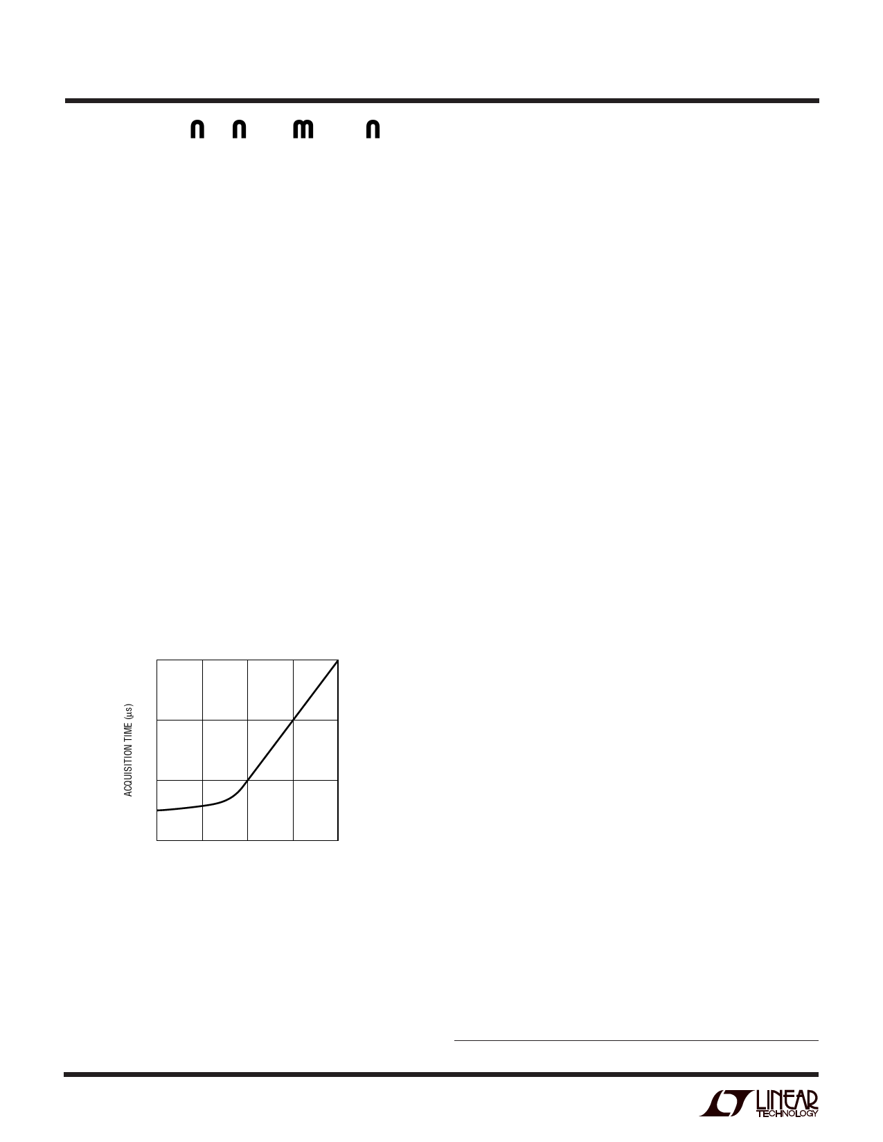
only a small leakage current. If the source impedance of
the driving circuit is low then the LTC1412 inputs can be
driven directly. As source impedance increases so will
acquisition time (see Figure 6). For minimum acquisition
time, with high source impedance, a buffer amplifier must
be used. The only requirement is that the amplifier driving
the analog input(s) must settle after the small current
spike before the next conversion starts (settling time must
be 50ns for full throughput rate).
10
1
0.1
0.01
10
100
1k
10k
100k
SOURCE RESISTANCE (Ω)
1412 F06
Figure 6. Acquisition Time vs Source Resistance
Choosing an Input Amplifier
Choosing an input amplifier is easy if a few requirements
are taken into consideration. First, to limit the magnitude
of the voltage spike seen by the amplifier from charging
the sampling capacitor, choose an amplifier that has a low
output impedance (<100Ω) at the closed-loop bandwidth
frequency. For example, if an amplifier is used in a gain of
1 and has a unity-gain bandwidth of 50MHz, then the
output impedance at 50MHz should be less than 100Ω.
The second requirement is that the closed-loop bandwidth
must be greater than 40MHz to ensure adequate small-
signal settling for full throughput rate. If slower op amps
are used, more settling time can be provided by increasing
the time between conversions.
The best choice for an op amp to drive the LTC1412 will
depend on the application. Generally applications fall into
two categories: AC applications where dynamic specifica-
tions are most critical and time domain applications where
DC accuracy and settling time are most critical. The
following list is a summary of the op amps that are suitable
for driving the LTC1412. More detailed information is
available in the Linear Technology Databooks and on the
LinearViewTM CD-ROM.
LT®1223: 100MHz Video Current Feedback Amplifier.
6mA supply current. ±5V to ±15V supplies. Low Noise.
Good for AC applications.
LT1227: 140MHz Video Current Feedback Amplifier. 10mA
supply current. ±5V to ±15V supplies. Low Noise. Best for
AC applications.
LT1229/LT1230: Dual and Quad 100MHz Current Feed-
back Amplifiers. ±2V to ±15V supplies. Low Noise. Good
AC specifications, 6mA supply current each amplifier.
LT1360: 50MHz Voltage Feedback Amplifier. 3.8mA sup-
ply current. ±5V to ±15V supplies. Good AC and DC
specifications. 70ns settling to 0.5LSB.
LT1363: 70MHz, 1000V/µs Op Amps. 6.3mA supply cur-
rent. Good AC and DC specifications. 60ns settling to
0.5LSB.
LT1364/LT1365: Dual and Quad 70MHz, 1000V/µs Op
Amps. 6.3mA supply current per amplifier. 60ns settling
to 0.5LSB.
Input Filtering
The noise and the distortion of the input amplifier and
other circuitry must be considered since they will add to
the LTC1412 noise and distortion. The small-signal band-
LinearView is a trademark of Linear Technology Corporation.
10
Share Link: 