RF2658PCBA Ver la hoja de datos (PDF) - RF Micro Devices
Número de pieza
componentes Descripción
Lista de partido
RF2658PCBA Datasheet PDF : 10 Pages
| |||
RF2658
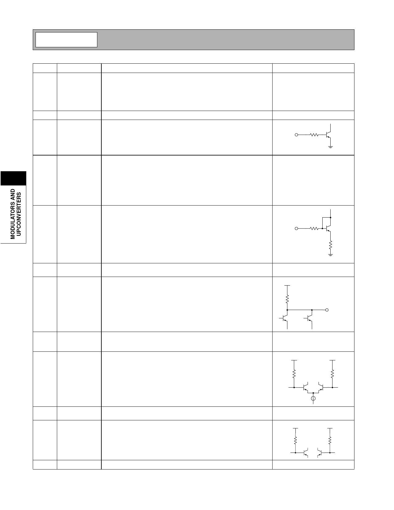
Pin Function Description
Interface Schematic
11
VCC3
Supply voltage for the AGC and the Bandgap circuitry. A 1nF external
bypass capacitor is required and an additional 0.1µF will be required if
no other low frequency bypass capacitors are nearby. The trace length
between the pin and the bypass capacitors should be minimized. The
ground side of the bypass capacitors should connect immediately to
ground plane. The part is designed to work from 2.7V to 3.3V supply.
12
GND1
Same as pin 6.
13
PD1
Power down control for overall circuit. When logic “high” (≥VCC-0.7V),
all circuits are operating; when logic “low” (<0.5V), all circuits are
10 kΩ
turned off. The input impedance of this pin is >10kΩ.
PD1
14
VCC4
Supply for the mixer stage only. The supply for the mixer is separated to
maximize IF to RF isolations and reduce the carrier leakage. A 100pF
external bypass capacitor is required and an additional 0.1µF will be
5
required if no other low frequency bypass capacitors are near by. The
trace length between the pin and the bypass capacitors should be min-
imized. The ground side of the bypass capacitors should connect
immediately to ground plane. The part is designed to work from 2.7V to
3.3V supply.
15
PD2
Power down control for mixer only. When connected to pin 10 (BG
OUT) the mixer circuits are operating; when connected to ground
(≤0.5V), the mixer is turned off but all other circuits are operating.
1 kΩ
PD2
450 Ω
16
GND2
Ground connection for the mixer stage. Keep traces physically short
and connect immediately to ground plane for best performance.
17
RF OUT RF output pin. An external shunt inductor to VCC plus a series blocking/
VCC4
matching capacitor are required for 50Ω output.
300 Ω
RF OUT
18
DEC
Current mirror decoupling pin. A 1000pF external capacitor is required
to bypass this pin. The ground side of the bypass capacitors should
connect immediately to ground plane.
19
LO2+
One half of the balanced mixer LO2 input. In single-ended applications,
BIAS
the other half of the input, LO2- is AC grounded. This is a 50Ω imped-
ance port. This pin is NOT internally DC blocked. An external blocking
capacitor (100pF recommended) must be provided if the pin is con-
40 Ω
nected to a device with DC present.
LO2+
BIAS
40 Ω
LO2-
20
21
22
5-64
LO2-
MIX IN-
MIX IN+
One half of the balance mixer LO2 input. In single ended applications,
this pin is AC grounded with a 100pF capacitor.
One half of the 200Ω balanced impedance input to the mixer stage.
This pin is NOT internally DC blocked. An external blocking capacitor
(2200pF recommended) must be provided if the pin is connected to a
device with DC present. If no IF filter is needed, this pin may be con-
nected to MOD OUT+ through a DC blocking capacitor. An appropriate
matching network may be needed if an IF filter is used.
See pin 19.
BIAS
100 Ω
MIX IN-
Same as pin 21, except complementary input.
See pin 21.
BIAS
100 Ω
MIX IN+
Rev A8 010720
Share Link: 