RF2658PCBA Ver la hoja de datos (PDF) - RF Micro Devices
Número de pieza
componentes Descripción
Lista de partido
RF2658PCBA Datasheet PDF : 10 Pages
| |||
RF2658
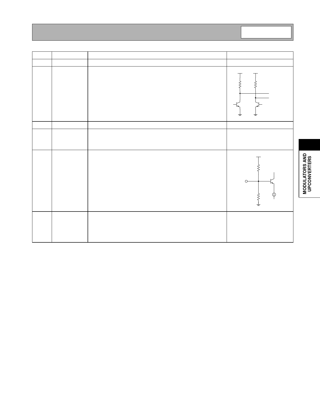
Pin
23
24
Function
GND2
MOD OUT-
Description
Interface Schematic
Same as pin 16.
One half of the balanced AGC output port. The impedance of this port
is 200Ω balanced. If no filtering is required, this pin can be connected
to the MIX IN- pin through a DC blocking capacitor. This pin requires an
inductor to VCC to achieve full dynamic range. In order to maximize
gain, this inductor should be a high-Q type and should be parallel reso-
nated out with a capacitor (see application schematic). This pin is NOT
DC blocked. A blocking capacitor of 2200pF is needed when this pin is
connected to a DC path. An appropriate matching network may be
needed if an IF filter is used.
VCC3
VCC3
100 Ω
100 Ω
MOD OUT-
MOD OUT+
25 MOD OUT+ Same as pin 24, except complementary output.
See pin 24.
26
DEC
AGC decoupling pin. An external bypass capacitor of 10nF capacitor is
required. The trace length between the pin and the bypass capacitors
should be minimized. The ground side of the bypass capacitors should
connect immediately to ground plane.
5
27
GC
Analog gain control for AGC amplifiers. Valid control voltage ranges are
from 0.5VDC to 2.5VDC. The gain range for the AGC is 88dB. These
voltages are valid ONLY for a 37kΩ source impedance.
BIAS
21 kΩ
GC
40 kΩ
28
VCC2
Supply for the modulator stage only. A 10nF external bypass capacitor
is required and an additional 0.1µF will be required if no other low fre-
quency bypass capacitors are nearby. The trace length between the pin
and the bypass capacitors should be minimized. The ground side of the
bypass capacitors should connect immediately to ground plane. The
part is designed to work from 2.7V to 3.3V supply.
Rev A8 010720
5-65
Share Link: 